Excerpt
Oscillatory transmission through non-tunneling regime of single rectangular tunnel barrier:
Parametric dependence of maxima and of minima
Md Mahmud Hasan and Sujaul Chowdhury
Chapter I Background on Quantum Mechanics
Chapter I Background on Quantum Mechanics
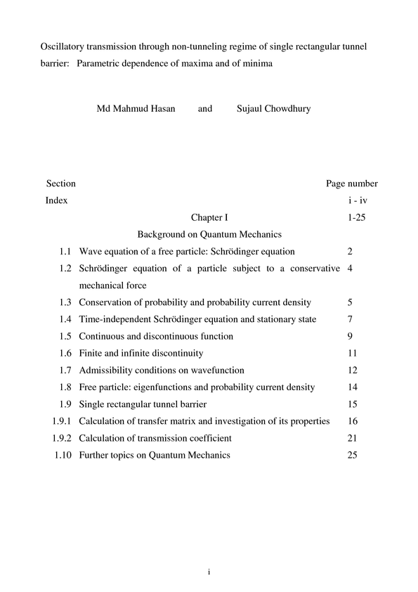
If we associate the wave packet
∞
1 ω − ) t kx ( i Ψ ³ = π dk e ) k ( a ) t , x (
2
∞ − ∞
1 ω − − ) t kx ( i ³ Ψ where a(k) = dx e ) t , x (
π 2 ∞ − with a free material particle, we can use de Broglie’s equations p = ! k and E = ω !
and rewrite the above two equations as ∞
1 ) k ( a ω − ) t kx ( i ! Ψ ³ = ) k ( d e ) t , x (
! π ! 2 ∞ − i ∞ − ) Et px ( 1 ) k ( a
! Ψ ³ or, = where a(p) = ! dp e ) p ( a ) t , x (
! π 2 ∞ − i ∞ − − ) Et px ( 1
! ³ Ψ or, a(p) = dx e ) t , x (
! π 2
∞ − In three dimensions & & i
− & & & ) Et r . p ( 1 ! Ψ ³ -----------(1.1) ) t , r ( = p d e ) p ( a
3 ! π ) 2 (
all momentum space
& & =
+ + where r . p z p y p x p
z y x Equation (1.1) gives i & & i p − & & Ψ ∂ = ) Et r . p ( x ! ! ³ p d e ) p ( a
∂ 3 ! π x ) 2 ( 2
p
x − & & i
− 2 & & Ψ ∂ ) Et r . p ( 2 ! ! ³ p d e ) p ( a = and
2 3 ! π ∂ ) 2 ( x 2
p
y − & & i
− 2 Ψ ∂ & & ) Et r . p ( 2 ! ! ³ p d e ) p ( a Similarly, =
2 3 ∂ ! π y ) 2 (
Oscillatory transmission through non-tunneling regime of single rectangular tunnel barrier:
Parametric dependence of maxima and of minima
Md Mahmud Hasan and Sujaul Chowdhury
. Hence equation (1.2) and (1.3) give For a free particle, E =
m
equation (1.4) is called wave equation or Schrödinger equation for a free particle. Equation (1.4) is a linear equation and hence a monochromatic wave such as & & i
− & ) Et r . p (
!
e ) p ( a as well as a wave packet given by equation (1.1) satisfy it.
Chapter I Background on Quantum Mechanics
1.2 Schrödinger equation of a particle subject to a conservative mechanical force
∂ * !
* Ψ Ψ Ψ Ψ ³ x ³ 1) A comparison of dx and < p > = dx < x > =
∂ x i shows that expectation value of momentum, < p > of a particle having wavefunction
Ψ associated with it can be computed in the same way as that of its position < x > if ∂ !
the operator is substituted in place of x. This statement introduces operator
i ∂ x
∂ !
formalism in quantum mechanics. Thus the operator of x is x, operator of p is .
i ∂ x
∂ !
By “operator of p is ”, we in fact mean, the operator we need to calculate
i ∂ x
∂ !
expectation value of p is .
i ∂ x
p 2
= E by the operator correspondence of p be obtained from the classical equation
m 2
∂ ∂ !
! respectively, and letting the operators operate on the and E as and i
∂ i ∂ t x
∂
! . wavefunction Ψ . Thus operator of E is i
∂ t
p 2
3) If a conservative force acts on a particle, total energy E = + V where V is
m 2 potential energy and hence V is a function of position only. Hence ∞ + ∞ +
Thus operator of V(x) is V(x).
Oscillatory transmission through non-tunneling regime of single rectangular tunnel barrier:
Parametric dependence of maxima and of minima
Md Mahmud Hasan and Sujaul Chowdhury
p 2
4) Using the operator correspondences of E, p and V, + V = E gives
m 2
This is the Schrödinger equation of a particle moving in a potential V. In three
1.3 Conservation of probability and probability current density Let us consider a particle under the action of a conservative mechanical force. The wave equation of the associated matter wave is given by the Schroedinger
where V is the potential associated with the force. Complex conjugate of equation
Multiplying equation (1.5) by * Ψ , we get
Chapter I Background on Quantum Mechanics
Equation (1.7) - (1.8)
· 2 * ! [ * Ψ ∂ Ψ ∂ §
¸ * ∇ Ψ − Ψ ∇ 2 * 2 Ψ − Ψ Ψ ] = i ! ¨ + Ψ
¸ ∂ ∂ © t m 2 t ¹
& * & • ( * & Ψ − Ψ ∇ 2 ! ∇ ∂ ( *
or, − Ψ ∇ Ψ ) = i ! Ψ Ψ )
∂ m 2 t
& • [ & Ψ − Ψ ∇ & * ! ( * ∂
2 ∇ Ψ ∇ Ψ )] = − Ψ or, -----------(1.9)
∂ mi 2 t
& • S & ∂ ρ
∇ = − or,
∂ t
& Ψ − Ψ ∇ & * & ! ( *
2 Ψ ∇ Ψ where ρ = Ψ ) and S = ----------(1.10)
mi 2 Equation (1.9)
& & ∂ ³ τ
³ τ • ∇ = − ρ d S d over a volume v.
∂ t
v v
& & ∂ ³ τ
³ • A = − ρ or, d S d ----------(1.11)
∂ t
v Using Gauss’s divergence theorem The surface integral is over the closed surface that encloses the volume v. In equation (1.11), ³ τ ρ d is probability of presence of a particle in the volume v.
v
∂ ³ τ
− ρ d is time rate of decrease of probability of presence of the particle in the
∂ t
v
& & &
volume v. Since this rate is equal to ³ • A , we can say that S d S is time rate of flowout of the probability per unit area through the surface enclosing the volume v. The
&
probability changes or decreases because of change of Ψ with time. Hence S is called probability current density. For a system of a large number of particles, < S > is average particle current density, i.e. number of particles crossing per unit time through a unit area perpendicular to the flow.
Oscillatory transmission through non-tunneling regime of single rectangular tunnel barrier:
Parametric dependence of maxima and of minima
Md Mahmud Hasan and Sujaul Chowdhury
1.4 Time-independent Schrödinger equation and stationary state Schrödinger equation for a particle under conservative force is
&
The Hamiltonian is also time independent. Equation (1.12) simplifies considerably.
& = u( r & ) f(t) as a solution of equation (1.12). u is a function
Let us try Ψ ) t , r ( of space coordinates only and f is a function of time only. Equation (1.12)
LHS of equation (1.13) is a function of position only and RHS of equation
& ) is a function of position only. Since
(1.13) is a function of time only, because V( r
space (coordinates) and time are independent (ignoring theory of relativity), equation (1.13) makes sense only if both sides of equation (1.13) are equal to a constant, say
&
( )
Chapter I Background on Quantum Mechanics
op eigenvalue equation of total energy. ∴ C is an eigenvalue of total energy (an observable). ∴C is real. Let us denote C by E.
2 ! & )] u( r & ) = E u( r & )
2 ∇ + V( r ∴Equation (1.16) [− --------(1.17a)
m 2
& ) = E u( r & )
H u( r or, --------(1.17b)
op Equation (1.17) is called time-independent Schroedinger equation. ∂ f(t) = E f(t) ) t ( Ef d f(t) = !
i ! Equation (1.15) or,
∂ i t dt 1 nt 1 ) nt 1 = 0 nt Let f(t) = nt e ∴ n nt or, (n − E ! e = 0 ∴n − E ! e ≠ 0 e = E ! e
i i i i
− Et iE = − i ω 1 = − ! e ω − e ! t i ∴ f(t) = or, n = E ! =
i i
− & , t) = u( r & ) f(t) & ) & ) Et e ω − e ! t i ∴ Ψ ( r = u( r = u( r ---------(1.18) i i *
− & & , t) Ψ ( r & , t) = u*( r & ) & ) & ) u( r & ) Et t E
2 e ! e ! = * Ψ ∴ Ψ ( r ) t , r ( u( r = u*( r E is real, ∴ E* = E.
&
2
= ) r ( u ---------(1.19) &
2 Ψ From equation (1.19), we find that ) t , r ( is independent of time. Thus the states
given by equation (1.18) are stationary states. Expectation value of any observable A is
& &
* τ Ψ Ψ < A > = ³ d ) t , r ( A ) t , r (
op i i * − & & t E Et
! ! * τ = ³ d ] e ) r ( u [ A e ) r ( u using equation (1.18)
op i i
− & & Et Et
! ! * τ = ³ E is real. d ) r ( u A e e ) r ( u
op If op A does not explicitly contain the variable t (time).
Oscillatory transmission through non-tunneling regime of single rectangular tunnel barrier:
Parametric dependence of maxima and of minima
Md Mahmud Hasan and Sujaul Chowdhury
& &
* τ = ³ d ) r ( u A ) r ( u
op For stationary states, expectation value of any observable A is independent of time, A itself does not depend explicitly on t. provided the operator op
e is a function of position 1
− In hydrogen atom, e.g., the potential V(r) =
πε r 4
0 2 Ψ for the only. Thus solution of equation (1.12) will give stationary state. Thus
electron and expectation values of all observables (e.g. energy) of the electron remain independent of time. This explains why hydrogen atom is stable; thus we get an explanation of one of the ad hoc assumptions of Bohr that the electron in hydrogen atom stays in stationary state.
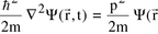
1.5 Continuous and discontinuous function
f(x)
x
df
f(x) above is a continuous function. It is single valued at every value of x.
dx is also continuous and single valued.
Chapter I Background on Quantum Mechanics
f(x)
x 0
x
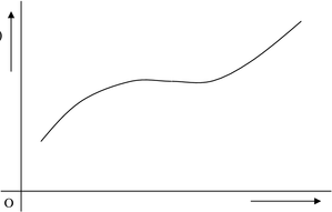
f(x) above is a discontinuous function of x. The discontinuity is at x = 0 x
where the function is many valued. f( 0 x ) is unspecified. 1 f < f( 0 x ) < 2 f . x − ∈) = 2 Lt ∈→ f( 0 f
0 Lt ∈→ f( 0 x +∈) = 1 f .
0
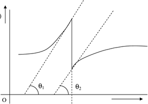
f(x)
x
x 0
df at x = 0
x − ∈ is tan 1 θ .
dx
Oscillatory transmission through non-tunneling regime of single rectangular tunnel barrier:
Parametric dependence of maxima and of minima
Md Mahmud Hasan and Sujaul Chowdhury
df at x = 0
θ . Here ∈ → 0. x +∈ is tan 2
dx
θ and 2 θ may or may not be equal, depending on the nature of f(x). Thus the
1 df may or may not be continuous.
derivative
dx df = tan 90° = ∞ .
At x = 0 x ,
dx
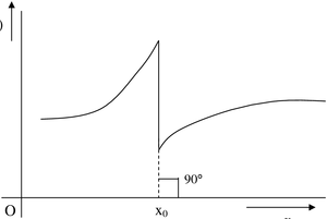
f(x)
x
1.6 Finite and infinite discontinuity f and 2 f The discontinuity considered above is finite discontinuity, because 1 x ) < b where either a or b (or both) is + ∞ or − ∞ , the are finite. If a < f( 0
discontinuity is infinite discontinuity.
Chapter I Background on Quantum Mechanics
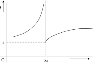
f(x)
x 0
x
Lt ∈→ f( 0 x +∈) = a
0
x − ∈) = + ∞ Lt ∈→ f( 0
0
x ) < ∞ . a < f( 0
1.7 Admissibility conditions on wavefunction
2 = 1 is finite. 1. Ψ (x , t) →0 as x → ± ∞ , because ³ τ Ψ d all space
2. Ψ (x , t) must be finite, single valued and continuous function of x for all time t; this is because of probability interpretation of Ψ .
Ψ ∂ is a continuous function of x, because otherwise Ψ ∂ = c where 1
3. c < c < 2 c at
∂ ∂ t t say x = 0 x .
Oscillatory transmission through non-tunneling regime of single rectangular tunnel barrier:
Parametric dependence of maxima and of minima
Md Mahmud Hasan and Sujaul Chowdhury

x
0
x
This means Ψ = c t which is many valued at x = 0 x . But Ψ must be single valued
according to condition (2).
Ψ ∂ must be continuous function of x if V(x , t) is continuous. Because: if V(x, t)
4.
∂ x
Ψ ∂ is also continuous (condition (3))
is continuous, V(x, t) Ψ (x, t) is continuous.
∂ t function of x. Hence Schroedinger equation 2 2 ! ∂ Ψ (x , t) +V(x , t) Ψ (x , t) Ψ ∂ t) (x,
= − i !
∂ 2 ∂ m 2 t x 2 2 Ψ ∂ is continuous function of x; otherwise Ψ ∂ Ψ ∂
gives is continuous. Thus
∂ 2 2 ∂ ∂ x x x
Ψ ∂
becomes infinite at points (x) where is discontinuous.
∂ x
Ψ ∂ must be continuous function of x if V does not have infinite discontinuity. In
5.
∂ x 2 2 ! Ψ ∂ = − Ψ ∂ ∂ Ψ + V(x, t) Ψ (x, t),
Schroedinger equation i ! is always
∂ ∂ 2 ∂ m 2 t t x
Chapter I Background on Quantum Mechanics
Ψ ∂ has any discontinuity say at x = x 0 , the
continuous function of x (condition 3). If
∂ x
everywhere, V is forced to be + ∞ at x = 0 x . Thus unless V has an infinite Ψ ∂ must be a continuous function of x.
discontinuity,
∂ x
Any finite discontinuity of V makes V Ψ finite discontinuous. This is adjusted
1.8 Free particle: eigenfunctions and probability current density
∂ V
V , force acting on the particle F(x) = − If the potential is constant, V(x) = 0
∂ x = 0; so the particle is free. 0 V can be taken to be zero, without any loss of generality. Time-independent Schroedinger equation is
i
− ) Et px ( ω − ! ∴ u(x) = A ikx ) t kx ( i ∴ Ψ (x , t) = A e e = A e
Oscillatory transmission through non-tunneling regime of single rectangular tunnel barrier:
Parametric dependence of maxima and of minima
Md Mahmud Hasan and Sujaul Chowdhury
k 2
Probability current density corresponding to the free particle eigenfunction i
− ) Et px (
! Ψ =A is e * ! [ Ψ ∂ Ψ ∂
* Ψ −Ψ S = ]
∂ ∂ mi 2 x x i i i i
− − ! − − ! − − ! [ * ∂ (A ∂ ( * ) Et px ( ) Et px ( ) Et px ( ) Et px (
! ! ) − A A )] = e e e e A
∂ ∂ mi 2 x x ! ! ! i p - (− ! i p)] = p k i p =
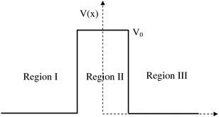
1.9 Single rectangular tunnel barrier
− a +a x (0, 0)
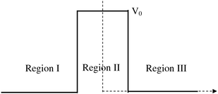
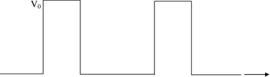
If we have variation of potential V(x) as shown in the above figure, we have a one-dimensional, single, rectangular potential barrier. If the width and height of the barrier are finite and small, we have a tunnel barrier of width 2a and height V 0 . The barrier is defined as x > V(x) = 0 for a + < < − for a x a = V 0
Chapter I Background on Quantum Mechanics
There are two finite discontinuities of V(x), one at x = −a and another at x = +a.
There are three regions as shown. According to the choice of origin, V(x) is zero in two of the three regions and is constant (V 0 ) in region II. We now proceed to obtain transfer matrix of the barrier and find its properties. We shall use waves and match them at the potential discontinuities using the boundary conditions described in section 1.7.
1.9.1 Calculation of transfer matrix and investigation of its properties (E < V 0 )
V(x)
− a +a x (0, 0) Solutions of time-independent Schrödinger equation 2 2 !
d + V(x)] u(x) = E u(x)
[−
2 m 2 dx 2
m 2 u d +
= − or, 0 u )) x ( V E (
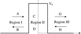
2 2 ! dx in the three regions are u 1 , u 2 and u 3 given by mE 2 − ikx ikx 2 + = = k Be Ae ) x ( u where
1
2 ! − ) E V ( m 2 β − β x x 2 0 + = = β De Ce ) x ( u where
2
2 ! − ikx ikx + = He Ge ) x ( u
3
The expressions for u 2 and β 2 imply that we are considering free electrons of kinetic
energy less than V 0 impinging on the barrier from the left.
Oscillatory transmission through non-tunneling regime of single rectangular tunnel barrier:
Parametric dependence of maxima and of minima
Md Mahmud Hasan and Sujaul Chowdhury
Using the boundary condition u 1 = u 2 at x = −a, we get − β β − ika ika Be a a De + + Ae = Ce ---------(1.20) Again, the boundary condition du du
2 1 = at x = −a gives
dx dx β − β − x x ikx ikx ikBe β − β at x = −a − ik Ae = De Ce β β − − a a ika ika ikBe − β − β Ae = De Ce or, ik ik ik − β β − ika ika a a De − − or, Be Ae = Ce ---------(1.21)
β β
The boundary condition u 2 = u 3 at x = +a gives β − β − a a De ika ika He + + Ce = Ge ---------(1.22) du du
3 2 = And at x = +a gives
dx dx β − β − x x ikx ikx ikHe β − β − De Ce = ikGe at x = +a β − β − a a ika ika ikHe β − β − => De Ce = ikGe β β
β − β − a a ika ika He − − => De Ce = Ge ---------(1.23)
ik ik From equation (1.20) + (1.21), we have ik ik − β − ika ika a − + + = Be ) 1 ( Ae ) 1 ( Ce 2
β β
ik 1 ik 1 β + β + − a ika a ika − + + = => Be ) 1 ( Ae ) 1 ( C
β β 2 2 From equation (1.20) − (1.21), we have
ik ik − β ika ika a + + − = Be ) 1 ( Ae ) 1 ( De 2
β β
ik 1 ik 1 β − β − − a ika a ika + + − = => Be ) 1 ( Ae ) 1 ( D
β β 2 2 Now in the form of matrix we can write
Chapter I Background on Quantum Mechanics
§ · ik 1 ik 1 β + β + − a ika a ika · § · § − + A C ¨ ¸ e ) 1 ( e ) 1 (
¸ ¨ ¸ ¨ β β 2 2 ¨ ¸
¸ ¨ ¸ ¨
¨ ¸ =
¸ ¨ ¸ ¨ ik 1 ik 1 β − β − − a ika a ika + − ¨ ¸ e ) 1 ( e ) 1 (
¸ ¸ ¨ ¨ ¸ ¸ ¨ ¨ β β 2 2 ¨ ¨ ¸ ¸
¹ © ¹ © B D
© ¹
From equation (1.22) + (1.23), we have
β β
β − β a a ika − + + = De ) 1 ( Ce ) 1 ( Ge 2
ik ik
β β 1 1 − β − − β ika a ika a − + + = => De ) 1 ( Ce ) 1 ( G
ik 2 ik 2
From equation (1.22) − (1.23), we have β β
β − β − a a ika + + − = De ) 1 ( Ce ) 1 ( He 2
ik ik
β β 1 1 + β − + β ika a ika a + + − = => De ) 1 ( Ce ) 1 ( H
ik 2 ik 2 Now in the form of matrix we can write
· § · § C G β β · § 1 1 − β − − β ¸ ¨ ¸ ¨ ika a ika a − + ¸ ¨ e ) 1 ( e ) 1 (
¸ ¨ ¸ ¨
ik 2 ik 2 ¸ ¨ =
¸ ¨ ¸ ¨
¸ ¨ β β 1 1 + β − + β ika a ika a ¸ ¸ ¨ ¨ ¸ ¸ ¨ ¨ + − ¸ ¨ e ) 1 ( e ) 1 (
¹ © ik 2 ik 2 ¹ © ¹ © D H
· § G β β · § 1 1 − β − − β ¸ ¨ ika a ika a − + ¸ ¨ e ) 1 ( e ) 1 (
¸ ¨
ik 2 ik 2 ¸ ¨ =
¸ ¨
¸ ¨ β β 1 1 + β − + β ika a ika a ¸ ¸ ¨ ¨ + − ¸ ¨ e ) 1 ( e ) 1 (
¹ © ik 2 ik 2 ¹ © H
· § · § A ik 1 ik 1 β + β + − a ika a ika ¸ ¨ − + ¸ ¨ e ) 1 ( e ) 1 (
β β ¸ ¨ 2 2 ¸ ¨
¸ ¨ ¸ ¨
ik 1 ik 1 β − β − − a ika a ika ¸ ¸ ¨ ¨ + − ¸ ¨ e ) 1 ( e ) 1 (
β β ¹ © 2 2 ¹ © B
§ · § · · § M M G A
12 11 ¨ ¨ ¸ ¸ ¨ ¨ ¸ ¸ ¸ ¸ ¨ ¨ = or, ---------(1.24)
© ¹ ¹ © © ¹ M M H B
22 21
Oscillatory transmission through non-tunneling regime of single rectangular tunnel barrier:
Parametric dependence of maxima and of minima
Md Mahmud Hasan and Sujaul Chowdhury
The M matrix is called transfer matrix. The elements of the matrix are calculated in the following.
β ik 1 1 β + − − β a ika ika a + + = e ) 1 ( e ) 1 ( M
11 β 2 ik 2 β ik 1 1 β − − − β − a ika ika a − − + e ) 1 ( e ) 1 (
β 2 ik 2 β β ik ik 1 − β − β ika 2 a 2 a 2 − − + + + = e ] e ) 1 )( 1 ( e ) 1 )( 1 [(
β β ik ik 4
β β ik ik 1 − β − β ika 2 a 2 a 2 + − − + + + + = e ] e ) 1 1 ( e ) 1 1 [(
β β ik ik 4 β ik 1 1 − β − β β − β ka 2 i a 2 a 2 a 2 a 2 − + + + = e ] 2 / ) e e )( ( ) e e ( [
β ik 2 2 β k i − ka 2 i β − + β = e ] a 2 sinh ) ( a 2 [cosh ----------(1.25)
β k 2
β ik 1 1 β + + β a ika ika a − − = e ) 1 ( e ) 1 ( M
22 β 2 ik 2 β ik 1 1 β − + β − a ika ika a + + + e ) 1 ( e ) 1 (
β 2 ik 2 β β ik ik 1 β − β ika 2 a 2 a 2 + + + − − = e ] e ) 1 )( 1 ( e ) 1 )( 1 [(
β β ik ik 4 β β ik ik 1 β − β ka 2 i a 2 a 2 + + + + + − − = e ] e ) 1 1 ( e ) 1 1 [(
β β ik ik 4
β ik 1 1 β − β β − β ka 2 i a 2 a 2 a 2 a 2 − + − + = e ] 2 / ) e e )( ( ) e e ( [
β ik 2 2 β ik 1 ka 2 i β + − β = e ] a 2 sinh ) ( a 2 [cosh
β ik 2 β k i ka 2 i β − − β = e ] a 2 sinh ) ( a 2 [cosh ----------(1.26)
β k 2
Chapter I Background on Quantum Mechanics
β ik 1 1 β + − β a ika ika a − + = e ) 1 ( e ) 1 ( M
12 β 2 ik 2 β 1 1 ik β − − β − a ika ika a + − + e ) 1 ( e ) 1 (
β ik 2 2
β β 1 ik ik β − β a 2 a 2 + − + − + = ] e ) 1 )( 1 ( e ) 1 )( 1 [(
β β ik ik 4 β β 1 ik ik β − β a 2 a 2 − − + + − + − = 1 [( 1 ( e ) 1 ] e ) 1
β β 4 ik ik β ik 1 β − β a 2 a 2 − − = 2 / ) e e )( (
β ik 2 β ik 1
β − = a 2 sinh ) (
β ik 2 β k i
β + − = a 2 sinh ) ----------(1.27) (
β k 2 β 1 1 ik β + − + β a ika ika a + − = M e ) 1 ( e ) 1 (
21 β ik 2 2 β 1 1 ik β − − + β − a ika ika a − + + e ) 1 ( e ) 1 (
β ik 2 2
β β 1 ik ik β − β a 2 a 2 − + + + − = ] e ) 1 )( 1 ( e ) 1 )( 1 [(
β β ik ik 4 β β ik ik 1 β − β a 2 a 2 − + − + − − + = ] e ) 1 1 ( e ) 1 1 [(
β β ik ik 4
β ik 1 β − β a 2 a 2 − − = 2 / ) e e )( (
β ik 2
β ik 1
β − = a 2 sinh ) (
β ik 2 β k i
β + = a 2 sinh ) ( ---------(1.28)
β k 2 We find that the elements of the transfer matrix M obey the following properties. * * M = = 22 M 11 M M , or ----------(1.29)
11 22 * * M = M = 12 M or, 21 M ----------(1.30)
21 12
Oscillatory transmission through non-tunneling regime of single rectangular tunnel barrier:
Parametric dependence of maxima and of minima
Md Mahmud Hasan and Sujaul Chowdhury
We now evaluate the determinant of the M matrix.

22 21
− = M M M M
21 12 22 11
* * − = M M M M
12 12 11 11 β β k i k i − ka 2 i ka 2 i β − + β β − − β = e ] a 2 sinh ) ( a 2 [cosh e ] a 2 sinh ) ( a 2 [cosh
β β k 2 k 2
β β k i k i
β + − β + − ] a 2 sinh ) ( [ ] a 2 sinh ) ( [
β β k 2 k 2 β β k 1 k 1 2 2 2 2 2 β + − β − + β = a 2 sinh ) ( a 2 sinh ) ( a 2 cosh
β β k 4 k 4
β β k k 1 2 2 2 2 β + − − + β = a 2 sinh ] ) ( ) [( a 2 cosh
β β k k 4
β k 1 2 2 β − + β = a 2 sinh ] 4 [ a 2 cosh
β k 4
2 2 β − β = a 2 sinh a 2 cosh
= 1 Thus

=
1
----------(1.31)
22 21
i.e. the determinant of the transfer matrix is unity.
1.9.2 Calculation of transmission coefficient
V(x)
−
a +a x (0 , 0)
Chapter I Background on Quantum Mechanics
We have solutions of time-independent Schrödinger equation 2 2 2 ! m 2 d + V(x)] u(x) = E u(x) u d +
= − [− or, 0 u )) x ( V E (
2 2 2 ! m 2 dx dx in the three regions given by u 1 , u 2 and u 3 mE 2 − ikx ikx 2 + = = Be Ae ) x ( u where k
1
2 ! − ) E V ( m 2 β − β x x 2 0 + = = β De Ce ) x ( u where
2
2 ! − ikx ikx + = He Ge ) x ( u .
3 To calculate transmission coefficient of the tunnel barrier, we need to recognize that A is amplitude of the plane wave incident on the barrier from the left. B is that of the wave reflected from the barrier. G is that of transmitted plane wave. H is that of the reflected wave (if any) in region III. We have equation (1.24) relating amplitudes of the four plane waves.
· · § § · § A M M G
12 11 ¸ ¸ ¨ ¨ ¸ ¨
= ¸ ¸ ¨ ¨ ¸ ¨
¸ ¸ ¨ ¨ ¸ ¨
B M M H ¹ ¹ © © ¹ ©
22 21 The matrix equation is equivalent to the following two equations.
11 + = B M A M G ---------(1.32)
12
21 + = and B M A M H . ---------(1.33)
22 To obtain an expression for transmission coefficient, we set H = 0 recognizing that we expect no reflection in region III. As such, equation (1.33) gives M
21 − = A B ---------(1.34)
M
22 which we can put in equation (1.32) to get − 1 M M M M M M
21 12 21 12 22 11 11 − = = = A A A ---------(1.35) A M G
M M M
22 22 22 using equation (1.31)
Oscillatory transmission through non-tunneling regime of single rectangular tunnel barrier:
Parametric dependence of maxima and of minima
Md Mahmud Hasan and Sujaul Chowdhury
2
G
T = . With the aid Now transmission coefficient of the single barrier is given by
1 2
A
1
T = of equation (1.35), T 1 reduces to ----------(1.36)
1 2
M
22 2
B
R = Reflection coefficient of the single barrier is given by .
1 2
A
With the aid of equation (1.34), R 1 reduces to 2
M
21 R = ---------(1.37)
1 2
M
22 2 = 21 T M ---------(1.38)
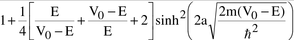
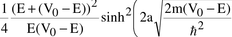
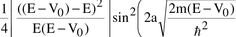
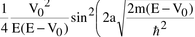
1 using equation (1.36). We now use equation (1.36) to obtain an analytic expression for T 1 for E < V 0 , The transmission coefficient is given by 1 1
T = =
1
2 *
22 M M M 22 22 1
=
β β k i k i − ka 2 i ka 2 i β − − β β − + β e ] a 2 sinh ) ( a 2 [cosh e ] a 2 sinh ) ( a 2 [cosh
β β k 2 k 2 using equation (1.26) 1 1
= =
β β k 1 k 1 2 2 2 2 2 2 β − + β β − + β + a 2 sinh ) ( a 2 cosh a 2 sinh ) ( a 2 sinh 1
β β k 4 k 4 1 1
= =
β 2 2 k 1 β 2 2 k 1 β − + + 2 a 2 sinh ] ) ( 1 [ 1 β − + + + a 2 sinh ] 2 4 [ 1 β k 4 2 2 β 4 k 1
= --------(1.39a)
β k 1 2 2 β + + a 2 sinh ) ( 1
β k 4
Chapter I Background on Quantum Mechanics
1
=
º ª 2 2 · § § β · k 1 2 » « + β + + ¸ ¨ ¸ ¨ a 2 sinh 2 1
β ¹ © » « ¹ © k 4
¼ ¬
1
=
!
¼ ¬ ¹ ©
0 1
=
· § 2
¸ +
1
¸
!
¹ ©
0 1
= --------(1.39b)
· § 2

¸ +
1
¸
!
¹ ©
0 Equation (1.39) is for E < V 0 . m 2 2 2 γ ± = β ∴ γ − = − − = β i For E > V 0 , ) V E (
0 2 !
= = = γ = β Using x tan i ix tanh , x cos ix cosh , x sin i ix sinh , i in equation (1.39a),
we get 1 1 = = T γ 1 γ k 1 i k 1 2 2 2 γ − − + 2 2 γ + + ) a 2 sin ( ) ( i 1 a 2 i sinh ) ( 1
γ γ k 4 k i 4 1
= ---------(1.40a)
γ k 1 2 2 γ − + ( a 2 sin ) 1
γ k 4 1
=
º ª 2 2 · § § γ · k 1 2 » « γ − + + ¸ ¨ ¸ ¨ a 2 sin 2 1
γ ¹ © » « ¹ © k 4
¼ ¬
1
=

!
¼ ¬ ¹ ©
0
Oscillatory transmission through non-tunneling regime of single rectangular tunnel barrier:
Parametric dependence of maxima and of minima
Md Mahmud Hasan and Sujaul Chowdhury
1
=
º ª · § 2
¸
+
1
¸
!
» « ¹ © ¼ ¬
0
1
= ---------(1.40b)
· § 2
¸
+
1
¸
!
¹ ©
0
γ + = β for transmission coefficient of the single barrier for E > V 0. We have chosen i ; γ − = β choosing i does not change the expression.
1.10 Further topics on Quantum Mechanics Further topics on Quantum Mechanics can be found in textbooks including reference [1].
Oscillatory transmission through non-tunneling regime of single rectangular tunnel barrier:
Parametric dependence of maxima and of minima
Md Mahmud Hasan and Sujaul Chowdhury
Background on Microelectronics
Chapter II Background on Microelectronics
2.1 Insulator and its band model
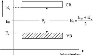
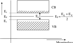
A number of allowed energy bands are completely filled and above these bands, there is a series of completely empty bands at 0 K. Between the highest filled band called valence band (VB) and the next empty band called conduction band (CB), the energy gap is large, of the order of 5 to 10 eV. As such it is not possible at practical temperatures to thermally excite and thereby take an appreciable number of electrons across the gap from near the top of VB (E v ) to near the bottom of CB (E c ). As such all the energy bands are either completely filled or completely empty at any practical temperature. If we apply an external electric field, there is no electron in CB to participate in electrical conduction. Electrons of completely filled VB cannot find any empty and allowed state nearby in energy to go to if their kinetic energy would increase by being accelerated by the electric field; hence electrons of VB cannot participate in electrical conduction. As such no observable electrical current is caused by applied electric field. All solids having such energy band model and such electrical conductivity are classified as insulator, example: diamond having band gap of 7 eV.
Higher
energy of electron
Meaningless
Figure 2.1: Band model of insulator (at 0 K). The energy gap E g is large and energy bands are narrow. Fermi energy for insulator at 0 K is given by E + E
v c
E F = ------------(2.1)
2
Oscillatory transmission through non-tunneling regime of single rectangular tunnel barrier:
Parametric dependence of maxima and of minima
Md Mahmud Hasan and Sujaul Chowdhury
i.e. E F lies halfway between VB and CB, and E F does not change much with change in temperature. So E F can be taken halfway between VB and CB for all practical temperatures.
2.2 Intrinsic semiconductor and its band model
Higher
energy of electron
Meaningless
Figure 2.2: Band model of intrinsic semiconductor (at non-zero K); VB is partially empty and CB is partially filled by electrons. But at 0 K, VB is completely filled by electrons and CB is completely empty as for insulators. Intrinsic semiconductor crystal contains atoms of one element only. For example, intrinsic Si crystal contains atoms of Si only. Band model of intrinsic semiconductors at 0 K is similar to that of insulators except that energy bands are broad and gaps are narrow. There is a wide, completely vacant conduction band separately by a narrow energy gap E g from a wide, completely filled valence band at 0 K. If we apply an external electric field, at 0 K, there is no electron in CB to participate in electrical conduction. Electrons of completely filled VB cannot find any empty and allowed state nearby in energy to go to if their kinetic energy would increase by being accelerated by the electric field. As such electrons of VB cannot participate in electrical conduction. As such no observable electrical current is caused by applied electric field, as in the case of insulators.
Chapter II Background on Microelectronics
But as temperature is raised from 0 K, electrons are thermally excited from near the top of VB (E v ) to near the bottom of CB (E c ) across the small energy gap E g . Thus we get appreciable number of electrons in CB which are free taking their effective mass into account. Number of free electrons in CB increases as temperature is raised further. Electrons that come to CB leave behind empty and allowed states called holes in VB. As such number of holes in VB is equal to number of electrons in CB for intrinsic semiconductors. If we apply an external electric field, at non-zero K, free electrons in CB gain kinetic energy by being accelerated and these electrons find empty and allowed states to go to, nearby in energy scale. Thus free electrons in CB can participate in electrical conduction and we get sufficient observable current which increases with increasing temperature because number of electrons in CB increases with increasing temperature. Because of holes, electrons of VB find empty and allowed states nearby in energy to go to as they gain kinetic energy by being accelerated by the electric field. As such electrons of VB can also participate in electrical conduction and give rise to observable electrical current in presence of applied electric field. We say that holes in VB contribute to electrical current. This current also increases with increasing temperature because number of holes in VB increases with increasing temperature, enabling larger number electrons of VB to go to empty states nearby in energy scale and thereby contribute to electrical current. Contribution of free electrons of CB and of atomic or bound or non-free electrons of VB to observable current add to each other because electrons of both CB and VB move in same direction in applied electric field. The two contributions are unequal, that of VB is smaller, although number of electrons in CB and number of holes in VB are equal. This is because mobility and drift velocity of non-free electrons of VB is smaller than those of free electrons of CB. Since electrons of CB and of VB move in same direction in applied electric field, holes of VB and electrons of CB move in opposite directions. Motion of free electrons in CB in one direction and motion of free holes of VB in opposite direction
Oscillatory transmission through non-tunneling regime of single rectangular tunnel barrier:
Parametric dependence of maxima and of minima
Md Mahmud Hasan and Sujaul Chowdhury
are equivalent in all physical effects except for the notorious Hall effect which shows Hall voltages of opposite polarity in the two cases as can be discerned using two separate crystals in one of which electrons of conduction band are majority carriers and in another of which holes of valence band are majority carriers. This leads one to consider holes as positively charged particles. Although holes are not bodily particles, it is possible to explain observable effects by considering holes as particles different from electrons and it is possible to bestow or associate not only positive charge but also effective mass with holes. Holes can be considered free taking their effective mass into account. Fermi energy of intrinsic semiconductor is given by * E 3 m g h + = E ------------(2.2) Log T k
e B F
* 4 2 m e where * m and *
m are effective mass of electron in CB and of hole in VB
e h E
g F = respectively. At T = 0 K, E , i.e. midway between VB and CB. In general
2 E g as T is increased above 0
* m > *
m , and hence Fermi level E F is slightly above
h e
2 K. Number of electrons n e in CB and number of holes n h in VB per unit volume of the crystal are equal and are given by 2 /
2 /
2 /
at 300 K whereas there are 10 22 atoms / cm 3 in Si crystal. It can be seen from
Chapter II Background on Microelectronics
equation (2.3), (2.4) and (2.5) that n e and n h increase rapidly as temperature is raised. Equation (2.2) to (2.5) hold provided E g >> k B T. This condition is satisfied by semiconductors like Si for which E g = 1.21 eV and for Ge for which E g = 0.78 eV
whereas k B T § 0.025 eV or 25 meV only at room temperature 300 K.
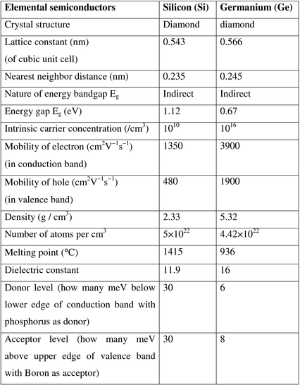
2.3 Elemental and compound semiconductors
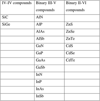
An elemental semiconductor contains atoms of one element only. Examples are silicon (Si), germanium (Ge) of column IV and selenium (Se) and Tellurium (Te) of column VI of periodic table. Various properties of Si and Ge are listed in Table 2.1. During early 1950s, Ge was the major semiconductor material. However it proved unsuitable for many applications, because electronic devices made of germanium exhibited high leakage current at only moderately elevated temperatures. Since early 1960s, Si has become a practical substitute virtually supplementing Ge as a material for semiconductor fabrication. Main reasons for these are: Si devices exhibit much lower leakage currents and high quality silicon dioxide (SiO 2 ) which is a very good insulator is easy to produce. Si, considered by many as a universal semiconductor material, cannot perform many important functions. Energy gap of Si is indirect and is small. It was natural to turn to other materials, notably compound semiconductor materials which offer many desired properties and can be synthesized without much difficulty. A compound semiconductor is composed of atoms of two elements. An example is GaAs (Gallium Arsenide, pronounced “gaas” for ease of frequent utterance) which consists of atoms of Ga and As. GaAs is a binary or two element compound semiconductor and is also called a III-V compound semiconductor as Ga comes from column III and As comes from column V of the periodic table of elements. Binary compound semiconductors are also made of elements of other columns of periodic table and are accordingly called II-VI semiconductors, IV-IV semiconductors. Table 2.2 shows a list of elements of different columns of periodic
Oscillatory transmission through non-tunneling regime of single rectangular tunnel barrier:
Parametric dependence of maxima and of minima
Md Mahmud Hasan and Sujaul Chowdhury
table which are used in obtaining compound semiconductors. A list of some compound semiconductors obtained using these elements are listed in Table 2.3.
Table 2.1: Properties of Si and Ge crystals at 300 K
Chapter II Background on Microelectronics
Table 2.2: A list of elements of different columns of periodic table which are used in obtaining compound semiconductors.
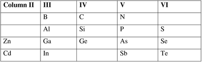
Table 2.3: A list of some compound semiconductors obtained using the elements listed in Table 2.2
that are absent in Silicon. Compound semiconductors especially gallium arsenide (GaAs) are used mainly for high speed electronic applications. Fluorescent materials such as those used in television screens usually are III-V compound semiconductors such as ZnS. Light detectors are made with InSb, CdSe. Semiconductor lasers are
Oscillatory transmission through non-tunneling regime of single rectangular tunnel barrier:
Parametric dependence of maxima and of minima
Md Mahmud Hasan and Sujaul Chowdhury
made by GaAs. Si and Ge cannot be used for laser because of its indirect bandgap. Laser action is possible in direct bandgap semiconductors because conservation of momentum of electron needs to be satisfied besides conservation of energy.
Table 2.4: Comparison of properties of elemental and binary semiconductors
We now describe advantages of GaAs. GaAs has some electronic properties which are superior to those of Si. It has a higher saturation electron velocity and higher electron mobility in conduction band, allowing it to function in high speed and high frequencies applications. Also, GaAs devices generate less noise than silicon devices. They can also be operated at higher power levels than equivalent silicon devices because they have higher breakdown voltages. These properties recommend
Chapter II Background on Microelectronics
GaAs circuitry in mobile phones, satellite communications, microwave and radar systems. Another advantage of GaAs is that it has a direct bandgap, which means that it can be used to emit light efficiently. Silicon has an indirect bandgap and so is poor in emitting light. Because of high switching speed, GaAs seems to be ideal for computer applications and for some time in 1980’s many thought that microelectronics market would switch from silicon to GaAs. We now describe advantages of Si. Silicon has three major advantages over GaAs. Firstly, Silicon is abundant and cheap to process. Silicon’s greater physical strength enables larger wafers (maximum of ~ 300 mm compared to ~150 mm diameter for GaAs). The second major advantage of Si is the existence of silicon dioxide (SiO 2 ) - one of the best insulators. Silicon dioxide can easily be incorporated onto silicon circuits and such layers are adherent to the underlying Si. GaAs does not form a stable adherent high quality insulating layer. The third and perhaps most important advantage of silicon is that it possesses a much higher hole mobility. This high mobility allows fabrication of higher speed p-channel field effect transistors, which are required for CMOS logic. Table 2.4 provides a comparison of properties elemental and binary compound semiconductors.
2.4 Alloy semiconductors: ternary and quaternary semiconductors
An attractive feature of binary compound semiconductors is that these can be combined or alloyed to form ternary (three element) or quaternary (four element) semiconductors called mixed crystal or alloy semiconductor. Melted mixture called solid solution of binary compound semiconductors can form ternary or quaternary alloy semiconductor after solidification. For example, a ternary III-V semiconductor A x B 1−x C is obtained after solidification of solid solution of binary compound semiconductors AC and BC. After solidification, A x B 1-x C is a ternary alloy semiconductor which consists of 100x atoms of element A and 100(1−x) atoms of element B randomly distributed in every 100 sites of group III sublattice. Atoms of element C occupy all the sites of group V sublattice. Value of x can be varied continuously between 0 and 1 (before
Oscillatory transmission through non-tunneling regime of single rectangular tunnel barrier:
Parametric dependence of maxima and of minima
Md Mahmud Hasan and Sujaul Chowdhury
solidification). A typical example is Al x Ga 1−x As (Aluminium Gallium Arsenide, pronounced algas for ease of frequent utterance), a ternary alloy semiconductor of great scientific and technological importance. In Al x Ga 1−x As, atoms of Al and Ga are randomly distributed in group III sublattice and atoms of As occupy all the sites of group V sublattice. Probability that a lattice point of group III sublattice is occupied by an Al atom is x and by a Ga atom is 1−x. In Al 0.3 Ga 0.7 As, probability that a lattice point of group III sublattice is occupied by an Al atom is 0.3 and by a Ga atom is 0.7, and probability that a lattice point of group V sublattice is occupied by an As atom is 1. Another form of ternary alloy is AB 1−y C y in which all the group III sublattice sites are occupied by atoms of element A and the sites of group V sublattice are randomly occupied by atoms of elements B and C. An example of this type of ternary alloy semiconductor is GaAs 1−y P y (Gallium Arsenide Phosphide, pronounced ga-asp) which is also technologically important and is obtained after solidification of solid solution of binary compound semiconductors GaAs and GaP. In similar manner, quaternary alloy semiconductors are formed by mixing atoms of four different elements. Such an alloy can consist of atoms of two group III elements A and B randomly distributed in group III sublattice sites and atoms of two group V elements C and D randomly distributed in group V sublattice sites to give the alloy A x B 1−x C y D 1−y . An example is In x Ga 1−x As y P 1−y (Indium Gallium Arsenide Phosphide, pronounced in-ga-asp). If atoms of three group III elements A, B, C randomly occupy group III sublattice sites and atoms of only one group V element D are present in group V sublattice sites, the quaternary alloy semiconductor A x B y C z D is formed. The composition is more conveniently expressed as (A x B 1−x ) y C 1−y D where x and y can be varied continuously between 0 and 1 (before solidification). An example is (In x Ga 1−x ) y Al 1−y As or In x Ga y Al z As (Indium Gallium Aluminium Arsenide, pronounced in-ga-alas).
Chapter II Background on Microelectronics
2.5 Bandgap engineering
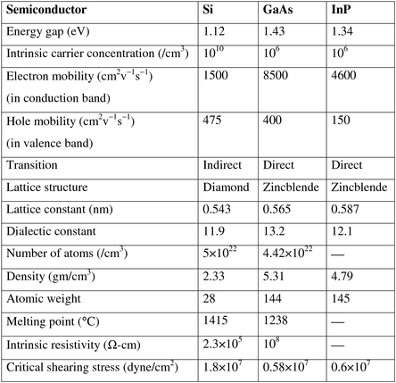
Bandgap engineering is the process of controlling or altering bandgap of a semiconductor crystal by controlling or changing composition of ternary or quaternary semiconductor alloys in solid solution before solidification. 1) Ternary or quaternary alloy semiconductors are made of two or three binary semiconductors in solid solution. 2) A ternary alloy semiconductor lies on tie line joining two binary semiconductors. For example, In x Ga 1−x As (Indium Gallium Arsenide, pronounced in-gas) lies on tie line between InAs and GaAs as shown in Figure 2.3. Bandgap E g of In x Ga 1−x As can be varied between E g of GaAs and E g of InAs by changing In content x between 0 and 1 in solid solution before solidification. Lattice constant a also changes as bandgap E g changes as is clear from Figure 2.3. 3) By choosing different binary compounds, it is possible to get ternary alloy of desired bandgap, because bandgap of ternary alloy lies between bandgap of the two end point binaries. 4) By choosing different binary compounds, it is possible to get ternary alloy of desired bandgap, because bandgap of ternary alloy lies between bandgap of the two end point binaries.
In x Ga 1−x As where 0 x 1
Lattice constant a
Figure 2.3: InGaAs lies on tie line between GaAs and InAs.
Oscillatory transmission through non-tunneling regime of single rectangular tunnel barrier:
Parametric dependence of maxima and of minima
Md Mahmud Hasan and Sujaul Chowdhury
Al x Ga 1−x As where 0 x 1
Lattice constant a
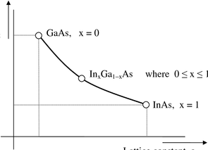
Figure 2.4: Al x Ga 1−x As lies on tie line between GaAs and AlAs.
Lattice constant (nm)
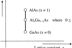
Figure 2.5: Bandgap engineering: on tie line between a pair of binary compounds lies the ternary.
5) By alloying, it is possible to vary bandgap continuously and monotonically by varying the composition. As another example, bandgap of ternary alloy Al x Ga 1−x As (0 x 1) depends on x. This bandgap can be varied continuously
and monotonically by varying Al content x of Al x Ga 1−x As. See Figure 2.4. Lattice constant remains almost unchanged in this case however.
Chapter II Background on Microelectronics
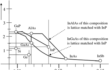
6) A more comprehensive look at different tie lines between different semiconductors is provided by Figure 2.5. The Figure provides a glimpse of the range of choice of end point binaries we have to obtain ternary of desired bandgap. We also understand how to get an alloy having lattice constant matched to GaAs or InP for example. We find that In x Ga 1−x As and In y Al 1−y As of particular compositions, namely for x = 0.53 and y = 0.52, are lattice matched to InP. This
can be seen more clearly in Figure 2.6.
Bandgap (eV)
0.60 0.65 0.55 Lattice constant (nm)
Figure 2.6: In 0.53 Ga 0.47 As (bandgap 0.74 eV) and In 0.52 Al 0.48 As (bandgap 1.45 eV) are lattice matched to InP.
7) An empirical relation usually gives bandgap E g of a ternary alloy A x B 1−x C semiconductor as a function of x. E g (x) = E g0 + bx + cx 2 -----------(2.6) where E g0 is bandgap of BC, the lower bandgap binary, E g0 + b + c is bandgap of AC, the upper bandgap binary, b is a fitting parameter and c is called bowing parameter which may be calculated theoretically or determined experimentally.
Oscillatory transmission through non-tunneling regime of single rectangular tunnel barrier:
Parametric dependence of maxima and of minima
Md Mahmud Hasan and Sujaul Chowdhury
2.6 Substrate and epitaxial layer
Single crystal semiconductors that are commonly used are of two categories: substrate or bulk crystal, and epitaxial layer. Substrate is a bulk piece of semiconductor crystal usually available as a circular piece around 0.5 mm in thickness and about 3 inch in diameter. For compound semiconductors, the only common substrates commercially available with relatively low defect density are of GaAs and of InP. Substrates of other compound semiconductors are usually not commercially available and needs to be grown as and when needed. Epitaxy is growth of a single crystal layer on top of a single crystal substrate of same or similar material. Here same or similar means same or similar crystal structure and equal or nearly equal lattice constant. ‘Epi’ means on and ‘taxy’ means arrangement, in Greek. Substrate crystal is first formed and then epitaxial layer is grown on it. Semiconductor electronic devices are often fabricated (made) within an extremely pure semiconductor crystal layer on top of a substrate. Epitaxial layer is used to get material characteristics superior to that in bulk crystal. This removes some of the stringent requirements on purity of substrate material. Substrate acts more like if not merely a supporting material and epitaxial layers serve as active region of electronic devices.
2.7 Semiconductor heterostructure and heterojunction
If an epitaxial layer of Si is grown on another epitaxial layer of Si or on a Si substrate, there is natural matching of crystal structure and lattice constant and high quality single crystal layers of any thickness can be grown without any problem. On the other hand, it is often desirable to obtain an epitaxial layer of one material say AlGaAs on an epitaxial layer of a different material say GaAs or on a substrate of different material say GaAs. This is known as hetero-epitaxy.
Chapter II Background on Microelectronics
space
space
Lower edge of CB
energy of
electron
Upper edge of VB
Figure 2.8: Band model of GaAs-AlGaAs heterostructure, E c > E v .
A semiconductor heterojunction is a junction of two different semiconductor crystals of unequal bandgap and this combination of semiconductors is called heterostructure, shown in Figure 2.7. Figure 2.8 shows band model of (undoped) GaAs-AlGaAs heterostructure having an abrupt heterojunction. The discontinuous in
valence band edge ¨E v and that in conduction band edge ¨E c are not in general equal, ¨E c : ¨E v is often taken as 65:35.
Fermi level of the un-GaAs layer is in the middle of bandgap of the un-GaAs layer; Fermi level of the un-AlGaAs layer is in the middle of bandgap of the un-AlGaAs layer. Since ¨E c > ¨E v , Fermi levels of the un-GaAs and the un-AlGaAs
Oscillatory transmission through non-tunneling regime of single rectangular tunnel barrier:
Parametric dependence of maxima and of minima
Md Mahmud Hasan and Sujaul Chowdhury
layers do not match on energy scale. E F of the un-AlGaAs layer is higher in energy (of electron scale) than E F of un-GaAs. This causes charge transfer; electrons transfer from CB of un-AlGaAs to CB of un-GaAs. Un-intentional donor ions of un-AlGaAs layer become uncovered and hence the un-AlGaAs layer, although intentionally undoped, contains a small amount of net +ive charge.
2.8 Further topics on Microelectronics
Further topics on Microelectronics: Physics and Processing can be found in e.g. reference [2].
Oscillatory transmission through non-tunneling regime of single rectangular tunnel barrier:
Parametric dependence of maxima and of minima
Md Mahmud Hasan and Sujaul Chowdhury
Background on Nanostructure Physics
Chapter III Background on Nanostructure Physics
3.1.1 Tunnel barrier: structure and band model
AlGaAs
(a)
E
c
of GaAs
E g of GaAs
E v of GaAs
E v of AlGaAs (b)
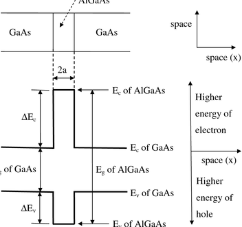
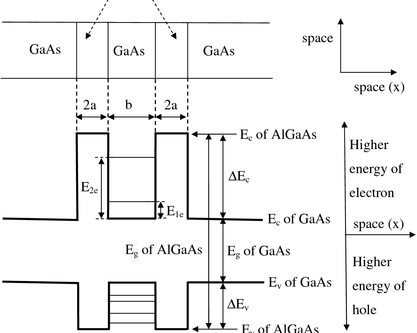
Figure 3.1 (a) Material structure and (b) band model of GaAs-AlGaAs tunnel barrier. E c is lower edge of conduction band and E v is upper edge of valence band. E g is bandgap. ΔE c is conduction band offset and ΔE v is valence band offset. We find a
tunnel barrier for electrons in CB and a tunnel barrier for holes in valence band. We often take ΔE c : ΔE v = 65: 35.
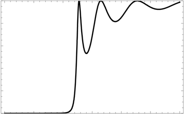
A simple example of tunnel barrier structure is provided by a thin layer of AlGaAs sandwiched between two thick layers of GaAs. Figure 3.1(a) shows material structure and Figure 3.1(b) shows band model of a tunnel barrier structure. There is a Δ rectangular potential barrier of height and width 2a for electrons in conduction E
c
Δ band (CB). There is a rectangular potential barrier of height and width 2a for E
v holes in valence band (VB). Width 2a of the barriers is nanometer scale or nanoscale (e.g. 10 nm) so that carriers can easily tunnel through the barriers giving rise to appreciable tunnel current. Hence the structure is called tunnel barrier. Rectangular
Oscillatory transmission through non-tunneling regime of single rectangular tunnel barrier:
Parametric dependence of maxima and of minima
Md Mahmud Hasan and Sujaul Chowdhury
tunnel barrier is used in textbooks of quantum mechanics to illustrate methods of calculation. But here we have a tunnel barrier in band model of a real nanostructure. If one of the two GaAs layers is appreciably n-doped, number of free electrons in CB of this GaAs layer is far more than number of free holes in VB. Then we forget the barrier in VB and consider tunneling of barrier in CB by free electrons. If one of the two GaAs layers is appreciably p-doped, number of free holes in VB of this GaAs layer is far more than number of free electrons in CB. Then we forget the barrier in CB and consider tunneling of barrier in VB by free holes. The barriers arise because E g of AlGaAs > E g of GaAs. E g of AlGaAs ~ E g of Δ + Δ . ΔE c ≠ ΔE v . ΔE c : ΔE v is often (not always) taken as 65: 35; GaAs = E E
v c Δ > Δ sometimes even 85: 15. The ratio is controversial, but E E . Carriers can feel
v c the barriers for their motion along x direction, i.e. for motion along the direction perpendicular to GaAs-AlGaAs interfaces. But carriers are free for motion parallel to the interfaces i.e. YZ plane.
3.1.2 Transport of electron or hole through tunnel barrier
We consider passage of electron from one side of barrier to the other; see Figure 3.2(a). In classical Physics, an electron in CB of GaAs having kinetic energy Δ E cannot enter into AlGaAs, let alone cross the AlGaAs layer. = total energy E <
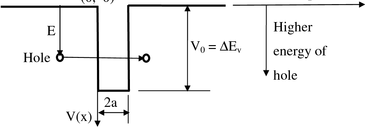
c If it enters into AlGaAs layer, its kinetic energy becomes negative which is absurd. Similar is the case with holes in VB; see Figure 3.2(b). A hole in VB of GaAs having Δ kinetic energy = total energy < E cannot enter into AlGaAs layer, because if it
v enters, its kinetic energy becomes negative which is also absurd. But if kinetic energy is larger than barrier height, there is a guarantee that the electron or hole will cross the AlGaAs layer and reach the GaAs layer on the other side of the barrier layer. This is because kinetic energy of carrier remains non-zero and positive throughout. Kinetic energy and total energy of carrier are equal outside the barrier layer because potential energy of carrier is zero outside barrier layer by choice of origin.
Chapter III Background on Nanostructure Physics
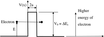
(a)
(0, 0) x space (x)
space (x) x (0, 0)
(b)
Figure 3.2 Figures to help describe transport of electron and of hole across tunnel barrier of height V 0 = ΔE c or ΔE v and width 2a for electrons in conduction band and
for holes in valence band respectively.
x (0, 0) space (x)
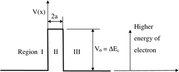
Figure 3.3 Figure to help describe tunneling of electron through a tunnel barrier of height V 0 = ΔE c and width 2a for electron in conduction band. Using Quantum mechanical analysis using validity of Born interpretation of Ψ
and using validity of Schroedinger equation everywhere including at the locations of finite potential discontinuities which give boundary conditions Ψ 1 = Ψ 2 and
Oscillatory transmission through non-tunneling regime of single rectangular tunnel barrier:
Parametric dependence of maxima and of minima
Md Mahmud Hasan and Sujaul Chowdhury
Ψ Ψ d d
2 1 = respectively at the finite potential discontinuity at x = 0; and Ψ 2 = Ψ 3
dx dx Ψ Ψ d d
3 2 = and respectively at the finite potential discontinuity at x = 2a, we can
dx dx get the following expressions for transmission coefficient T of a particle of (effective) mass m through the rectangular tunnel barrier of height V 0 and width 2a as 1
= T , for E > V 0 ------------(3.1)
2
V 1 2 0 α + ) a 2 ( sin 1
− ) V E ( E 4
0 1
= T , for E < V 0 ------------(3.2)
2
V 1 2 0 β + ) a 2 ( sinh 1
− ) E V ( E 4
0
− ) V E ( m 2
2 0 = α where ------------(3.3)
2 ! − ) E V ( m 2
2 0 = β and ------------(3.4)
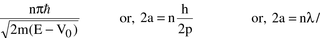
2 ! Here E is total energy of an electron which is same everywhere, i.e. conserved or constant of motion. E is kinetic energy of carriers outside the barrier. This is the same as total energy of carrier outside barrier because potential energy of carrier outside barrier is zero by choice of origin. Equation (3.2) becomes Equation (3.1) if we raise E from less than V 0 to greater than V 0 . Equation (3.1) becomes equation (3.2) if we reduce E from greater than V 0 to less than V 0 . Hence we can use any one of equation (3.1) and equation (3.2) to plot T as function of E for E ranging from 0 to above V 0 and we get what is shown in Figure 3.4(a) and (b). In principle, we should use equation (3.2) to plot T versus E curve for E < V 0 i.e. up to the point A in Figure 3.4(a); and we should use equation (3.1) to plot T versus E curve for E > V 0 i.e. beyond the point A. There are several significant features of the curve. 1) For E = 0, T = 0.
Chapter III Background on Nanostructure Physics
2) T can be non-zero even if kinetic energy of carrier outside the barrier is less than
barrier height V 0 . This we find in Figure 3.4(a) which shows that T is non-zero for E
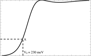
< V 0 where V 0 = 230 meV. We say that carriers tunnel through the barrier. 3) A particle having kinetic energy outside the barrier (E) greater than barrier height V 0 can cross the barrier, but there is no guarantee (T ≠ 1) unless 2a = nλ/2 where n =
1, 2, 3, … i.e. unless barrier width 2a is integral multiple of half of de Broglie h h
= = λ wavelength of electron inside the barrier layer. The condition
− p ) V E ( m 2
0 2a = nλ/2 comes from equation (3.1) which gives T = 1 for sin2aα = 0 or 2aα = nπ where n = 1, 2, 3, …; we exclude n = 0 on physical ground although it holds mathematically. 2 2 2 − π ! ) V E ( m 2 n 2 2 2 2 0 π = = n a 4 a 4 or, 2aα = nπ or,
− 2 ! ) V E ( m 2
0
= a 2 or, 2
0
0.0 0.2 0.4 0.6 0.8 1.0
1.0 1.0
0.8 0.8
0.6 0.6 T
0.4 0.4 0.2 0.2
0.0 0.0
0.0 0.2 0.4 0.6 0.8 1.0
E +eV/ (a)
Oscillatory transmission through non-tunneling regime of single rectangular tunnel barrier:
Parametric dependence of maxima and of minima
Md Mahmud Hasan and Sujaul Chowdhury
0.0 0.1 0.2 0.3 0.4 0.5 0.6
1.0 1.0
0.8 0.8
0.6 0.6 T
0.4 0.4
0.2 0.2
0.0 0.0
0.0 0.1 0.2 0.3 0.4 0.5 0.6
E +eV/ (b)
Figure 3.4 Transmission coefficient T of a rectangular tunnel barrier of height V 0 = 230 meV and width (a) 2a = 5 nm and (b) 2a = 15 nm as a function of energy E of an electron of effective mass 0.067m e of conduction band of GaAs. 4) T versus E curve is oscillatory and spectacular for higher energy of incident particle and for larger width of the tunnel barrier as we find in Figure 3.4(b).
λ = 5) The condition 2 / n a 2 can be given an interesting form as follows. nh h nh λ = 0 = − n a a 2 2 / n a 2 gives or, or, ) V E ( m 2 or,
− p 2 a 4 ) V E ( m 2 2
0 2 2 2 2 2 2 ! π ! ! n 4 n 2 2 2 = π = − π = − 4 ) V E ( m 2 n 4 ) V E ( or,
0 0
2 2 2 m 2 a 16 a 16 m 2 a 16 2 2 § π ! ·
2 2 = − = − ¸ ¨ n ) V E ( or, or, E n ) V E (
0 0 1 ¹ © a 2 m 2 where E 1 is ground state energy of a particle in a 1D box of width 2a. Thus 2 λ = = − 2 / n a 2 for T = 1 is equivalent to E n ) V E ( . Thus width of barrier is
0 1 integral multiple of half of de Broglie wavelength of electron inside the barrier is
Chapter III Background on Nanostructure Physics
equivalent to saying that kinetic energy of carrier inside barrier is integral square multiple of ground state energy of a particle in a 1D box of width 2a. Figure 3.4(a) and (b) can be obtained using the following program written in Mathematica 6.0. m=0.067*9.1*10^-31 hcut=(6.626*10^-34)/(2*3.1416) V0=0.230 a=5*10^-9
alpha=Sqrt[2*m*(X-V0)*1.6*10^-19/hcut^2] T=1/(1+0.25*V0^2*(Sin[alpha*a])^2/(X*(X-V0))) Plot[T,{X,0,1},PlotRange->{0,1},Frame->True,PlotStyle ->{{Thick,Black}},FrameTicks->All,FrameLabel->{"E (eV)","T"}] We now note several uses of tunnel barrier. 1) We can study fundamental Physics of transport of carriers across the barrier. 2) We can use it as part of i.e. as basic building block of other nanostructures. 3) We can put a tunnel barrier at entrance of carrier channel in nanostructures to allow high energy carriers enter into the channel.
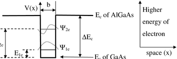
3.2 Quantum Well (QW)
Quantum well is opposite of tunnel barrier. A simple example of QW structure is provided by a thin layer of GaAs sandwiched between two thick layers of AlGaAs. Figure 3.5(a) shows structure and Figure 3.5(b) shows band model of the QW structure. There is a QW for electrons in CB and there is a QW for holes in VB. They trap free electrons and free holes respectively. Figure 3.6 shows electronic structure of QW for electrons in CB. E 1e , E 2e are discrete allowed values of kinetic energy as well as total energy (because potential energy V of electron inside the QW is zero by choice of origin) of electron in the QW for motion only along x direction i.e. perpendicular to GaAs-AlGaAs interfaces. E 1e , E 2e are called confined energy levels and associated states (Ψ ie ’s) are called bound states. This is because tails of associated wavefunctions do not penetrate far into
Oscillatory transmission through non-tunneling regime of single rectangular tunnel barrier:
Parametric dependence of maxima and of minima
Md Mahmud Hasan and Sujaul Chowdhury
AlGaAs barrier layers and hence an electron in such energy level cannot go far from the QW. The electron essentially remains confined in the QW.
GaAs
(a)
E
c
of AlGaAs
E g of AlGaAs
space (x) E v of AlGaAs (b)
Figure 3.5(a) Material structure and (b) band model of GaAs-AlGaAs Quantum Well (QW). E c is lower edge of conduction band and E v is upper edge of valence band. E g is bandgap. ΔE c is conduction band offset and ΔE v is valence band offset.
There is a QW for electrons in CB and there is a QW for holes in valence band. We often take ΔE c : ΔE v = 65: 35.
Values of E 1e , E 2e are calculated in textbooks on Quantum Mechanics; [thorough and complete details can be found in ISBN: 978-3-8383-7746-9]; the values of E 1e , E 2e depend on width b and depth ΔE c of QW. Exact value of ΔE c is not known; we take it 773x meV for GaAs-Al x Ga 1−x As QW. ΔE c ≈ 234 meV for GaAs-Al 0.3 Ga 0.7 As QW. Hence calculated values of E 1e , E 2e are approximate values.
Chapter III Background on Nanostructure Physics
E 2e
E c of GaAs
(0, 0) x
Figure 3.6 Figure showing electronic structure of QW for electrons in conduction band. E 1e , E 2e are allowed values of kinetic energy as well as total energy of electron for motion only along x direction i.e. perpendicular to GaAs-AlGaAs interfaces inside the QW. Potential energy is zero inside the QW by choice of origin. Space part of Ψ 1e and of Ψ 2e associated with E 1e , E 2e are shown by dotted curves. Tails of Ψ 1e and of Ψ 2e extend outside the QW to some extent.
Figure 3.7 (a) and (b) show parametric variations of E 1e , E 2e , E 3e , E 4e for electron in QW in conduction band. There are several features of the parametric variations. If we keep QW depth fixed, and increase QW width b, we find in Figure 3.7(a) that values of confined energy levels E ie ’s rapidly decrease; higher energy level decreases faster; number of confined energy levels that is accommodated within the depth of QW increases; the energy levels come closer to each other in energy scale. And if we keep QW width b fixed and increase QW depth by increasing Al content x of Al x Ga 1−x As, we find in Figure 3.7(b) that values of confined energy levels E ie ’s slowly increase; higher energy levels increase faster; number of confined energy levels that is accommodated within the depth of QW increases. Thus electronic structure of QW can be tuned by choosing QW width b and Al content x of Al x Ga 1−x As and hence value of QW depth during material growth.
Oscillatory transmission through non-tunneling regime of single rectangular tunnel barrier:
Parametric dependence of maxima and of minima
Md Mahmud Hasan and Sujaul Chowdhury
0.3
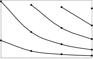
(a)
0.25
0.2
ie (eV)
0.15
E
0.1
0.05
0
5 1 0 1 5 2 0
QW w idth b (nm )
0.3
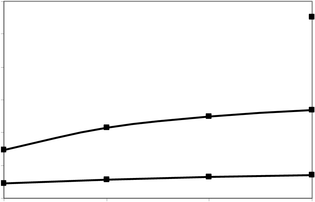
(b)
0.25
0.2
ie (eV)
0.15
E
0.1
0.05
0
0.1 0.2 0.3 0.4
Al content x of Al x Ga 1-x As
Figure 3.7 Parametric variations of confined energy levels E ie ’s of electron of effective mass 0.067m e in GaAs-Al x Ga 1−x As QW in CB. (a) Variation of E 1e , E 2e , E 3e and E 4e as function of QW width b = 5 to 20 nm for fixed Al content x = 0.4 corresponding to fixed QW depth 773x meV ≈ 310 meV. (b) Variation of E 1e and E 2e
as function of Al content x = 0.1 to 0.4 of Al x Ga 1−x As corresponding to QW depth 773x meV ≈ 77 to 310 meV for fixed QW width b = 10 nm.
Chapter III Background on Nanostructure Physics
In infinitely deep QW approximation, ΔE c → ∝ and we have a 1D potential
box of width b for motion along x direction, i.e. for motion perpendicular to GaAs- interfaces. Allowed values of kinetic energy as well as of total energy of an electron of effective mass *
m for motion along x direction are then given by
e º ª
Minimum allowed value of kinetic energy or total energy of electron for motion along x direction in the QW is E 1e . Hence E 1e is the lowest possible value of grand total energy of an electron in QW if values of kinetic energy of electron for motion along y and z directions are zero. The energy range from E c of GaAs to E c of GaAs + E 1e in the QW is completely forbidden. Band model shows variation of E c and of E v along the direction perpendicular to GaAs-AlGaAs interfaces i.e. variation of E c and E v as function of position along x direction. As such, carriers in QW are not free along x direction. But carriers in QW are free for motion parallel to interfaces i.e. in y and z directions. Thus carriers in QW are free in 2D, not 3D. Hence an electron system residing in QW is twodimensional electron system (2DES) or two-dimensional electron gas (2DEG). In infinitely deep QW approximation, i.e. for ΔE c → ∝,
º ª
motion along x direction is nearly continuous and carriers in QW are free in all three dimensions; we get 3DEG instead of 2DEG. Nothing in the well remains quantized; we do not call the well a Quantum Well; we call it classical well or potential well. > The well is Quantum Well if , i.e. if energy difference T k E ~ E + B ne e ) 1 n ( between consecutive energy levels is more than thermal broadening. Since
Oscillatory transmission through non-tunneling regime of single rectangular tunnel barrier:
Parametric dependence of maxima and of minima
Md Mahmud Hasan and Sujaul Chowdhury
º ª
AlGaAs QW at 300 K. Hence QW width must be small if it is to show quantization of energy of electron and resulting behaviour.
space (x) (0, 0) x
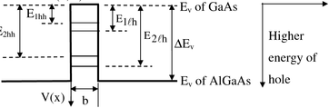
E 2hh
Figure 3.8 Figure showing electronic structure of QW for holes in valence band. Allowed values of kinetic energy as well as total energy are E 1hh , E 2hh for heavy hole; E " for light hole for motion only along x direction inside the QW. Potential E " ,
h 1 h
Figure 3.8 shows electronic structure of QW for holes in VB. In infinitely º ª
are two types of holes: light hole and heavy hole; * m can be * m or *
m " for heavy
h hh h hole and for light hole respectively. Hence we get two sets of confined energy levels in QW for holes in VB, as shown in Figure 3.8.
Chapter III Background on Nanostructure Physics
3.3 Symmetric double barrier
AlGaAs
(a)
E v of AlGaAs (b)
Figure 3.9 (a) Material structure and (b) band model of GaAs-AlGaAs symmetric double barrier. E c is lower edge of conduction band and E v is upper edge of valence band. E g is bandgap. ΔE c is conduction band offset and ΔE v is valence band offset. We often take ΔE c : ΔE v = 65: 35. There are two tunnel barriers separated by a QW
for electrons in CB; there are two tunnel barriers separated by a QW for holes in valence band. Energy levels E 1e , E 2e etc. in the QWs are also shown; these are allowed values of kinetic energy of carrier inside the non-isolated QWs for motion only along x direction i.e. for motion perpendicular to GaAs-AlGaAs interfaces. Figure 3.9(a) shows structure and Figure 3.9(b) shows band model of symmetric double barrier structure. The two AlGaAs layers are identical in width and in Al content. There are two tunnel barriers of equal height and equal width separated by a QW for electrons in CB, and there are two tunnel barriers of equal height and equal width separated by a QW for holes in VB. This means the two AlGaAs layers
Oscillatory transmission through non-tunneling regime of single rectangular tunnel barrier:
Parametric dependence of maxima and of minima
Md Mahmud Hasan and Sujaul Chowdhury
must be thin (~10 nm) and the GaAs layer between them must also have small width (~10 nm). The Quantum wells are non-isolated QWs. An allowed energy state in such a QW is quasi-bound state, because an electron in the QW can tunnel through either tunnel barrier and thus go out of the QW never to return. If an electron dwells for time τ in the QW, the quasi-bound energy levels E 1e , E 2e etc. in the QW acquire some ! . This is different from any thermal broadening which is of the order of
width ΔE ~ τ
k B T.
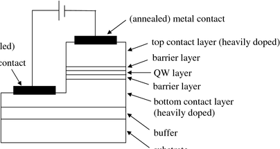
(a)
(annealed)
metal contact substrate
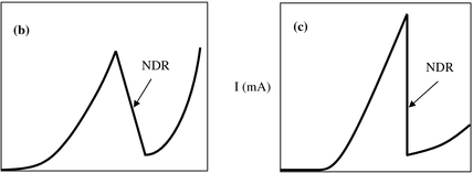
I
V (Volt)
V (Volt)
Figure 3.10 (a) A practical way of realising double barrier structure, called resonant tunneling diode. I-V characteristics at (b) room temperature, (c) low temperature.
Chapter III Background on Nanostructure Physics
An important application of double barrier structure is in resonant tunneling diode. A practical way of realising it is shown in Figure 3.10(a) while typical I-V characteristics are as shown in Figure 3.10(b) for room temperature and in Figure 3.10(c) for low temperature. It has negative differential resistance (NDR) behaviour. Double barrier structure has got a lot of applications based on its NDR behaviour.
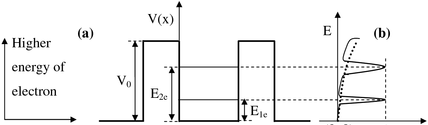
(0, 0) 1 T space (x) x (0 , 0)
Figure 3.11(a) Band model of a double barrier structure. (b) Thin curve shows transmission coefficient T of symmetric double barrier as a function of energy E of electron incident on left hand tunnel barrier. Dotted curve shows transmission coefficient T 1 of a single tunnel barrier in tunneling regime 0 < E < V 0 . We now describe transmission coefficient T of symmetric double barrier by an electron as function of total energy E of the electron incident normal to GaAs-AlGaAs interface of the left hand tunnel barrier. Let us consider an electron impinging on the double barrier from the left at an energy E; see Figure 3.11(a). E is kinetic energy of an electron outside the barriers. E is also total energy of an electron because potential energy of electron is zero outside the barriers by choice of origin. The probability that the incident electron passes through the two barriers is transmission coefficient T shown by thin curve in Figure 3.11(b). Figure 3.11(b) also includes, as dotted curve, transmission coefficient T 1 of a single barrier as a function of E in tunneling regime: 0 < E < V 0 . For most values of E, T is roughly equal to product of transmission coefficients of the two individual barriers: T § T L T R § 2
T . Both T L and T R are small,
1 i.e. << 1 for tunneling regime (0 < E < V 0 ) for typical barriers and hence the product T L T R is smaller still. Thus T is usually small. But a distinctive feature called resonant tunneling is that T rises to much higher values than T L T R for values of energy E of
Oscillatory transmission through non-tunneling regime of single rectangular tunnel barrier:
Parametric dependence of maxima and of minima
Md Mahmud Hasan and Sujaul Chowdhury
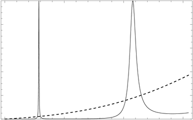
incident electron equal to or close to those of quasi-bound energy levels E 1e , E 2e , etc. in the non-isolated QW between the two barriers; in a structure having two identical barriers, there is perfect transmission (T = 1) for E = E 1e , E 2e , etc., called resonance, however small T L and T R may be; this is shown in Figure 3.11(b). For example, even if T 1 = 0.1 for E = E 1e , T will be equal to 1 for E = E 1e . Also indicated in Figure 3.11(b) is that full-width-at-half-maximum (FWHM) is larger for transmission peak at higher energy. We now express T as a function of E quantitatively.
V(x)
−2a (0, 0) b b+2a x Figure 3.12 Figure to help express transmission coefficient quantitatively. Here we have two identical rectangular tunnel barriers having a QW between them. Figure 3.12 shows two identical rectangular tunnel barriers having a QW between them. Transmission coefficient [thorough and complete calculations can be found in ISBN: 978-3-8383-7570-0] is given by 2
T
1 = ) E ( T ------------(3.6)
2 2 θ − + − + ] ) b a 2 ( k [ cos ) T 1 ( 4 T
1 1 for tunneling regime, i.e. for 0 < E < V 0 . Here 2a is width of each tunnel barrier, b is width of the QW between the two barriers,

= k ------------(3.7) !
T 1 is transmission coefficient of each tunnel barrier for 0 < E < V 0 , given by 1
= ------------(3.8) ) E ( T
1
2
V 1 2 0 β + ) a 2 ( sinh 1
− ) E V ( E 4
0
Chapter III Background on Nanostructure Physics

= β
------------(3.9) where
V 0 is height of each tunnel barrier = depth of the QW between the two tunnel barriers, m is effective mass of electron ª º · §
Off resonance, the cosine term in equation (3.6) is non-zero. T is minimum if cos 2 = θ − + π = θ − + 1 ] ) b a 2 ( k [ which gives n ) b a 2 ( k where n = 1, 2, 3, … . Hence
order of product of transmission coefficients of two individual tunnel barriers i.e. apart from the factor of 4, transmission appears to be cascaded transmission of two successive identical tunnel barriers, independent of width and depth of the quantum well between them. Resonant transmission peaks occur if the cosine term in equation (3.6)
(3.13) is also obeyed by quasi-bound energy levels of the non-isolated QW between the two barriers; [rigorous verification of this can be found in Dash, Samad, Chowdhury; monograph to be published 2012]. Thus values of energy E for resonance peaks are equal to values of energy of quasi-bound energy levels of the non-isolated QW formed between the two tunnel barriers. Pronounced transmission
Oscillatory transmission through non-tunneling regime of single rectangular tunnel barrier:
Parametric dependence of maxima and of minima
Md Mahmud Hasan and Sujaul Chowdhury
of electron occurs if energy E of an electron incident on the left hand tunnel barrier matches with energy of any of the quasi-bound energy levels of the non-isolated QW between the two barriers. Figure 3.13(a) compares, for electron in CB, transmission coefficient T of symmetric rectangular double barrier with transmission coefficient T 1 of one of the two single barriers in the tunneling regime: 0 < E < V 0 . We find that T 1 does not rise to more than 0.4, but T rises up to 1 at resonance. For the resonances at E 1e and E 2e , T 1 ≈ 0.025 and 0.2 respectively while T = 1. This is resonant tunneling. Figure 3.13
can be obtained using the following program in Mathematica 6.0.
a=2.5*10^-9 b=10*10^-9 x=0.2 V0=0.773*x m=0.067*9.1*10^-31 hcut=6.626*10^-34/(2*3.1416) k=Sqrt[2*m*X*1.6*10^-19/hcut^2] beta=Sqrt[2*m*(V0-X)*1.6*10^-19/hcut^2] theta=-ArcTan[0.5*(k/beta-beta/k)*(Tanh[2*beta*a])]+2*k*a T1=1/(1+0.25*V0^2*(Sinh[2*a*beta])^2/(X*(V0-X))) T=T1^2/(T1^2+4*(1-T1)*(Cos[k*(2*a+b)-theta])^2) Plot[{T1,T},{X,0,V0},PlotRange->{0,1.0}, PlotStyle->{{Dashed,Black},{Black}},Frame->True, FrameLabel->{"E (eV)","T"},PlotStyle->{Black}] Plot[Log[10,T],{X,0,V0},Frame->True, FrameLabel->{"E (eV)","Log 10 T"},PlotStyle->{Black}]
Chapter III Background on Nanostructure Physics
1.0
(a) 0.8
0.6 T 0.4
0.2
0.0
0.00 0.05 0.10 0.15
E +eV/

0
(b)
1
2 10 T
3
Log
4
5
6
0.00 0.05 0.10 0.15
E +eV/ Figure 3.13 (a) T versus E plot for electron of effective mass 0.067m e in conduction band of symmetric rectangular double barrier for the energy range 0 < E < V 0 for tunnel barrier width 2a = 5 nm, QW width b = 10 nm and Al content x = 0.2 of Al x Ga 1−x As. Dashed curve shows transmission coefficient T 1 of one of the two single barriers as a function of E in tunneling regime. (b) The T versus E plot on Log scale to reveal the rapid variations slowly.
Oscillatory transmission through non-tunneling regime of single rectangular tunnel barrier:
Parametric dependence of maxima and of minima
Md Mahmud Hasan and Sujaul Chowdhury
Some other notable features in Figure 3.13 are as follows. 1) Shape of resonance peaks is close to Lorentzian function.
2) Transmission coefficient is unity at resonances and falls off rapidly with energy on either side of resonances.
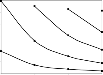
3) Full-width-at-half-maxima (FWHM) of resonant transmission peak is larger for the peak at higher energy. Parametric variations of values of energy E for which resonant transmission peaks occur are shown in Figure 3.14(a), (b) and (c); [thorough and complete details can be found in ISBN: 978-3-8383-7570-0]. The parameters are width 2a of each tunnel barrier, width b and depth of the QW between the two tunnel barriers. The depth is taken as 0.773x eV where x is Al content of Al x Ga 1−x As. Since values of energy E of quasi-bound levels of the non-isolated QW are equal to values of energy E for which resonant transmission peaks occur, the parametric variations shown in Figure 3.14 are also parametric variations of quasi-bound energy levels E 1e , E 2e , E 3e , … of the non-isolated QW between the two tunnel barriers.
0.3
(a) 0.25
0.2
i (eV)
0.15
E 0.1
0.05
0
5 1 0 1 5 2 0
w idth b of QW (nm )
Chapter III Background on Nanostructure Physics
0.3
(b) 0.25
0.2 i (eV)
0.15
E 0.1
0.05
0
0.1 0.2 0.3 0.4
Al content x of Al x Ga 1-x As
0.3
(c)
0.25
0.2 i (eV)
0.15
E
0.1
0.05
0
2 4 6 8 1 0
w idth 2a of each tunnel barrier (nm )
Figure 3.14 Parametric variation of values of energy E = E 1 < E 2 < E 3 < … for which resonant transmission peaks occur. The parameters are width 2a of each tunnel
barrier, width b and depth of the QW between the two tunnel barriers. The depth is
taken as 0.773x eV where x is Al content of Al x Ga 1−x As. (a) 2a = 10 nm, x = 0.4, (b) b = 10 nm, 2a = 6 nm, (c) b =15 nm, x = 0.3. These are also parametric variations of quasi-bound energy levels E ie ’s of non-isolated QW between the two tunnel barriers.
Oscillatory transmission through non-tunneling regime of single rectangular tunnel barrier:
Parametric dependence of maxima and of minima
Md Mahmud Hasan and Sujaul Chowdhury
There are several notable features of the parametric variations. See Figure 3.14(a); if we increase QW width b, keeping QW depth and tunnel barrier width 2a fixed, we find the following.
1) Values of quasi-bound energy levels E 1e , E 2e , E 3e , … which are also values of energy E for which resonant peaks occur go to lower values of energy E. 2) E 1e ~ E 2e etc. decrease i.e. energy separation between neighbouring quasi-bound energy levels of the non-isolated QW decreases; energy separation between neighbouring resonant transmission peaks also decreases.
3) Number of quasi-bound energy levels of the non-isolated QW also increases, i.e. number of transmission peaks in the tunneling regime 0 < E < V 0 increases. 4) As a transmission peak goes to lower energy E, its FWHM decreases; because FWHM is smaller for transmission peak at lower energy E. There are some more striking features of the parametric variations. See Figure 3.14(b); if we increase QW depth or tunnel barrier height by raising Al content x of Al x Ga 1−x As, keeping QW width b and tunnel barrier width 2a fixed, we find the following.
1) Values of energy E for which transmission peaks occur and hence values of quasibound energy levels E 1e , E 2e , E 3e , … of the non-isolated QW between the two tunnel barriers rise slowly.
2) Values of energy of higher energy quasi-bound levels rise more rapidly i.e. values of energy E of higher energy transmission peaks rise more rapidly. 3) Number of quasi-bound energy levels of the non-isolated QW also increases, i.e. number of transmission peaks in the tunneling regime 0 < E < V 0 increases. The most striking feature of the parametric variations is revealed by Figure 3.14(c); if we increase tunnel barrier width 2a keeping QW width b and depth fixed, we find that values of energy for which resonant transmission peaks occur i.e. values of quasi-bound energy levels E 1e , E 2e , E 3e , … in the non-isolated QW remain unchanged, although tunnel barrier width 2a appears at 5 places in the expression for transmission coefficient i.e. in equation (3.6). One more thing to note is that investigations show that as tunnel barrier width 2a is increased, FWHM of
Chapter III Background on Nanostructure Physics
transmission peaks decrease; this is expected in that rise in tunnel barrier width increases lifetime τ of carriers in the QW as the carriers in QW finds it difficult to ! of quasi-bound energy levels decreases;
leak out of QW, and hence width ΔE ~ τ
width of transmission peak is expected to be equal to width of quasi-bound energy levels in the QW.
3.4 Further study of Nanostructure Physics
For further study of Nanostructure Physics, one can read e.g. reference [2].
Oscillatory transmission through non-tunneling regime of single rectangular tunnel barrier:
Parametric dependence of maxima and of minima
Md Mahmud Hasan and Sujaul Chowdhury
Analytical calculation
Chapter V Transmission of electron through non-tunneling regime of single rectangular tunnel barrier:
Analytical calculation
4.1 Description of the problem
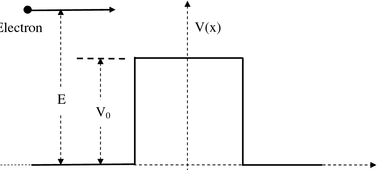
Electron
− a (0, 0) + a x Figure 4.1 A single rectangular tunnel barrier being traversed by an electron in nontunneling regime Figure 4.1 shows a single rectangular tunnel barrier of width 2a and height V 0 being traversed by an electron of total energy E > V 0 . Tunnel barrier was introduced in section 3.1.1 and 3.1.2. Width 2a of the barrier is nano-scale, e.g. 10 nm and height V 0 is typically 300 meV. The material outside the barrier layer on two sides is virtually infinite in thickness; in practice, the thickness is said to be semi-infinite and is very much larger than tunnel barrier width 2a. In this chapter, we shall calculate transfer matrix and transmission coefficient of the tunnel barrier for an electron in non-tunneling regime. This is a 1D problem.
4.2 Calculation of transfer matrix of single rectangular tunnel barrier
According to the choice of origin, see Figure 4.2, V(x) is zero in region I and III and is V 0 in region II. Solutions of time-independent Schrödinger equation 2 2 2 ! − )) x ( V E ( m 2 d + V(x)] u(x) = E u(x) u d
= + 0 u [− or, for E > V(x)
2 2 2 ! m 2 dx dx in the three regions are given by mE 2 − 2 ikx ikx = + = k Be Ae ) x ( u where
1 2 ! − ) V E ( m 2 γ − γ 2 x i x i 0 = γ + = De Ce ) x ( u where
2 2 !
Oscillatory transmission through non-tunneling regime of single rectangular tunnel barrier:
Parametric dependence of maxima and of minima
Md Mahmud Hasan and Sujaul Chowdhury
− ikx ikx + = He Ge ) x ( u
3
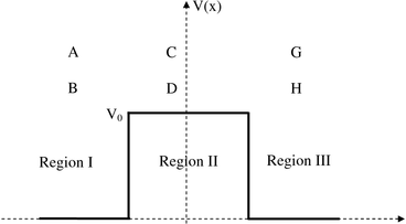
− a x + a (0 , 0)
Figure 4.2 Figure to help calculate transfer matrix of single rectangular tunnel barrier for non-tunneling regime. The expressions for u 2 and for γ 2 imply that we are considering a free electron
of total energy E > V 0 i.e. kinetic plus potential energy greater than V 0 traversing the barrier from the left hand side. E is a constant of motion; E is entirely kinetic in region I and III, but E −V 0 is kinetic energy of an electron in region II. The solutions ω − t i = Ψ for time-dependent Schroedinger equation is given by e ) x ( u ) t , x ( which are Ψ stationary states. u(x) is space part of ) t , x ( . − ikx ikx ikx + = We recognise that Ae in Be Ae ) x ( u is space part of the
1 wavefunction incident on the barrier from left hand side i.e. from region I. And Be − − ikx ikx ikx + = is space part of the wavefunction reflected from in Be Ae ) x ( u
1 ikx the potential discontinuity at x = −a back to region I. We also recognise that Ge of − ikx ikx + = He Ge ) x ( u is space part of wavefunction transmitted to region III after
3
completion of traversal through region II. Since there is no potential variation in He − = ikx
region III, there should be no reflection of u 3 in region III. As such we take 0, and hence H = 0.
Chapter V Transmission of electron through non-tunneling regime of single rectangular tunnel barrier:
Analytical calculation at x = −a, we get u = According to boundary condition 1 u
2
γ − γ − x i x i ikx ikx + = + at x = −a De Ce Be Ae γ γ − − a i a i ika ika + = + or, De Ce Be Ae -----------(4.1) du du
2 1 = at x = −a gives And boundary condition
dx dx γ − γ − x i x i ikx ikx x − = γ − γ = − at a De i Ce i ikBe ikAe γ γ − − a i a i ika ika γ − γ = − or, De i Ce i ikBe ikAe k k γ γ − − a i a i ika ika − = − De Ce Be Ae or, -----------(4.2)
γ γ u = x + = , we get Again, according to boundary condition at 2 u a
3
− γ − γ ikx ikx x i x i + = + He Ge De Ce at x = +a − γ − γ ika ika a i a i + = + or, He Ge De Ce -----------(4.3) du du
3 2 = x + = And boundary condition at gives a
dx dx − γ − γ ikx ikx x i x i x + = − = γ − γ at a ikHe ikGe De i Ce i − γ − γ ika ika a i a i − = γ − γ or, ikHe ikGe De i Ce i

− γ − ika ika a i − = He Ge De or, -----------(4.4) From equation (4.1) + (4.2), we get k k − γ − ika ika a i − + + = Be ) 1 ( Ae ) 1 ( Ce 2
γ γ
k 1 k 1 γ + γ + − a i ika a i ika − + + = Be ) 1 ( Ae ) 1 ( C or, -----------(4.5)
γ γ 2 2 From equation (4.1) −(4.2) we get
k k − γ ika ika a i + + − = Be ) 1 ( Ae ) 1 ( De 2
γ γ
k 1 k 1 γ − γ − − a i ika a i ika + + − = Be ) 1 ( Ae ) 1 ( D or, -----------(4.6)
γ γ 2 2 From equation (4.3) + (4.4) we get
Oscillatory transmission through non-tunneling regime of single rectangular tunnel barrier:
Parametric dependence of maxima and of minima
Md Mahmud Hasan and Sujaul Chowdhury

γ − a i ika + = De ) 1 ( Ge 2
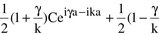
− γ −
ika a i
=
De ) G
or, -----------(4.7)
From equation (4.3) − (4.4) we get

γ − − a i ika − = De ) 1 ( He 2

+ γ −
ika a i
=
De ) H
or, -----------(4.8) In matrix form, equation (4.5) and (4.6) can be written as
· § k 1 k 1 γ + γ + − a i ika a i ika − + · § · § ¸ ¨ A C e ) 1 ( e ) 1 (
¸ ¨ ¸ ¨ γ γ 2 2 ¸ ¨
= ¸ ¨ ¸ ¨ -----------(4.9) ¸ ¨
k 1 k 1 γ − γ − − ¸ ¨ ¸ ¨ a i ika a i ika + − ¸ ¨ e ) 1 ( e ) 1 ( B D ¹ © ¹ ©
γ γ ¹ © 2 2
In matrix form, equation (4.7) and (4.8) can be written as γ γ · § 1 1 − γ − − γ · § · § ika a i ika a i + − G C ¸ ¨ e ) 1 ( e ) 1 ( ¸ ¨ ¸ ¨
k 2 k 2 ¸ ¨ = ¸ ¨ ¸ ¨ ----------(4.10)
¸ ¨ γ γ 1 1 + γ − + γ ¸ ¨ ¸ ¨ ika a i ika a i − + ¸ ¨ e ) 1 ( e ) 1 ( H D ¹ © ¹ ©
¹ © k 2 k 2 Equation (4.9) and (4.10) give γ γ · § 1 1 − γ − − γ § · ika a i ika a i − + G ¸ ¨ e ) 1 ( e ) 1 ( ¨ ¸
k 2 k 2 ¸ ¨ = ¨ ¸
¸ ¨ γ γ 1 1 + γ − + γ ¨ ¸ ika a i ika a i + − ¸ ¨ e ) 1 ( e ) 1 ( H © ¹
¹ © k 2 k 2
· § 1 1 k k γ + γ + − a i ika a i ika − + § · ¸ ¨ A e ) 1 ( e ) 1 (
¨ ¸ γ γ 2 2 ¸ ¨
¨ ¸
¸ ¨
k 1 k 1 γ − γ − − ¨ ¸ a i ika a i ika + − ¸ ¨ e ) 1 ( e ) 1 ( B © ¹
γ γ ¹ © 2 2 ----------(4.11)
· § § § · · T T A G
12 11 ¸ ¸ ¨ ¨ ¨ ¨ ¨ ¨ ¸ ¸ ¸ ¸ = ----------(4.12) or,
© © ¹ ¹ ¹ © T T B H
22 21
Equation (4.11) and (4.12) give
Chapter V Transmission of electron through non-tunneling regime of single rectangular tunnel barrier:
Analytical calculation
γ γ k 1 1 k 1 1 γ − − − γ − γ + − − γ a i ika ika a i a i ika ika a i − + + + = − e ) 1 ( e ) 1 ( e ) 1 ( e ) 1 ( T
11 γ γ 2 k 2 2 k 2 γ γ k 1 k 1 γ − − − γ − γ + − − γ a i ika ika a i a i ika ika a i + − − + + + + = e ) 1 1 ( e ) 1 1 (
γ γ k 4 k 4
γ − γ a 2 i a 2 i − γ e e k 1 1 − γ − γ ka 2 i a 2 i a 2 i + + + = e )] )( ( ) e e ( [
γ 2 k 2 2 γ k i − ka 2 i γ + + γ = e ] a 2 sin ) ( a 2 [cos ----------(4.13)
γ k 2
γ γ k 1 1 k 1 1 γ − + γ − γ + + γ a i ika ika a i a i ika ika a i + + + − − = e ) 1 ( e ) 1 ( e ) 1 ( e ) 1 ( T
22 γ γ 2 k 2 2 k 2 γ · § γ k 1 k 1 + γ − + γ ka 2 i a 2 i ka 2 i a 2 i + + + + + − − = ¸ ¸ ¨ ¨ e ) 1 1 ( e 1 1
γ γ ¹ © k 4 k 4
γ a 2 i γ − a 2 i − γ e e k 1 1 γ − γ ka 2 i a 2 i a 2 i + − + = e )] )( ( ) e e ( [
γ 2 k 2 2 γ k i ka 2 i γ + − γ = e ] a 2 sin ) ( a 2 [cos ----------(4.14)
γ k 2
∗
T = Thus 11 T
22
γ γ k 1 1 k 1 1 γ − − γ − γ + − γ a i ika ika a i a i ika ika a i + − + − + = e ) 1 ( e ) 1 ( e ) 1 ( e ) 1 ( T
12 γ γ 2 k 2 2 k 2
· § γ γ k 1 k 1 γ − γ a 2 i a 2 i − + − + − − + = ¸ ¨ e ) 1 1 ( e 1 1
γ γ ¹ © k 4 k 4
γ − γ a 2 i a 2 i − γ e e k 1
− = ) )( (
γ 2 k 2
γ k i
γ − = a 2 sin ) (
γ k 2 ----------(4.15)
Oscillatory transmission through non-tunneling regime of single rectangular tunnel barrier:
Parametric dependence of maxima and of minima
Md Mahmud Hasan and Sujaul Chowdhury
γ γ k 1 1 k 1 1 γ − − + γ − γ + − + γ a i ika ika a i a i ika ika a i + + + − = − e ) 1 ( e ) 1 ( e ) 1 ( e ) 1 ( T
21 γ γ 2 k 2 2 k 2
· § γ · § γ k 1 k 1 γ − γ a 2 i a 2 i − − + + − − + ¸ ¨ ¸ ¨ = e 1 1 e 1 1
γ γ ¹ © ¹ © k 4 k 4 γ − γ a 2 i a 2 i − γ e e k 1
− = ) )( (
γ 2 k 2 γ k i
γ − = a 2 sin ) (
γ k 2 γ − k i
γ − = a 2 sin ) ( ----------(4.16)
γ k 2 * T = Thus 12 T
21 We now evaluate determinant of the transfer matrix T; see Equation (4.12).

− =
Using equation (4.13) to (4.16) in , we get
T T T T
21 12 22 11
22 21

* *
− =
− =
T T T T
T T T T
12 12 11 11 21 12 22 11
22 21
γ γ k i k i − ka 2 i ka 2 i γ + − γ γ + + γ = e ] a 2 sin ) ( a 2 [cos e ] a 2 sin ) ( a 2 [cos
γ γ k 2 k 2 γ − γ k i k i
γ − γ − − ] a 2 sin ) ( ][ a 2 sin ) ( [ using equation (4.13) and (4.15)
γ γ k 2 k 2 2 γ γ k 1 k i 2 2 2 2 2 γ − − γ + − γ = a 2 sin ) ( a 2 sin ) ( a 2 cos
γ γ k 4 k 4
γ γ k k 1 2 2 2 2 γ − − + + γ = a 2 sin ] ) ( ) [( a 2 cos
γ γ k k 4
γ k 1 2 2 2 2 γ + γ = γ + γ = a 2 sin a 2 cos a 2 sin . . 4 . a 2 cos
γ k 4 = 1

− =
Thus = 1 ---------(4.17)
T T T T
21 12 22 11
22 21 i.e. determinant of the transfer matrix is unity.
Chapter V Transmission of electron through non-tunneling regime of single rectangular tunnel barrier:
Analytical calculation
4.3 Calculation of transmission coefficient of single rectangular tunnel barrier for non-tunneling regime
− a x + a (0 , 0)
Figure 4.3 Figure to help calculate transmission coefficient of single rectangular tunnel barrier for non-tunneling regime. We follow procedure of section 1.9.2. To calculate transmission coefficient of the barrier, we set H = 0 in equation (4.12) to get
§ § · · § · A T T G
12 11 ¨ ¨ ¸ ¸ ¨ ¸
= ¨ ¨ ¸ ¸ ¨ ¸ ---------(4.18)
¨ ¨ ¸ ¸ ¨ ¸
B T T 0 © © ¹ ¹ © ¹
22 21 The matrix equation (4.18) is equivalent to the following two equations. 11 + = ---------(4.19) B T A T G
12
21 + = and . ---------(4.20) B T A T 0
22 T
21 − = Equation (4.20) gives A B ---------(4.21)
T
22 Using equation (4.21) in equation (4.19), we get

= =
11
− = =
A T A T G A . Thus
12
T T A T T
22 22 22 22 using equation (4.17)
Oscillatory transmission through non-tunneling regime of single rectangular tunnel barrier:
Parametric dependence of maxima and of minima
Md Mahmud Hasan and Sujaul Chowdhury
2

=
) E ( T
Transmission coefficient is given by ------------(4.22)
22 2
T We now obtain an expression for .
22 2 * = T T T
22 22 22
γ γ k i k i − ka 2 i ka 2 i γ + + γ γ + − γ = e ] a 2 sin ) ( a 2 .[cos e ] a 2 sin ) ( a 2 [cos
γ γ k 2 k 2 2 γ k i 2 2 2 γ + − γ = using equation (4.14) a 2 sin ) ( a 2 cos
γ k 4 2 2 γ k 1 2 2 γ + + + γ = a 2 sin ) 2 ( a 2 cos
2 2 γ 4 k 2 2 γ k 1 2 2 γ + + + γ − = a 2 sin ) 2 ( a 2 sin 1
2 2 γ 4 k 2 2 2 2 γ γ k 1 k 1 2 2 γ − + + + = γ − + + = a 2 sin ] 1 ) 2 ( a 2 sin ) 2 [ 1 ( 1
2 2 2 2 γ γ 4 4 k k γ k 1 2 2 γ − + = ---------(4.23) a 2 sin ) ( 1
γ 4 k Using equation (4.23) in equation (4.22), we get 1
T =
2
T
22 1
= for E > V 0 ---------(4.24) T
γ k 1 2 2 γ − + a 2 sin ) ( 1
γ 4 k 1
=
− V E E 1 2 0 γ − + + a 2 sin ) 2 ( 1
− 4 E V E 0 1
=
2 2 − − − + ) V E .( E . 2 ) V E ( E 1 2 0 0 γ + 1 a 2 sin ] [
− 4 ) V E ( E
0
Chapter V Transmission of electron through non-tunneling regime of single rectangular tunnel barrier:
Analytical calculation 1
=
2 + − ) V E E ( 1 0 2 γ + a 2 sin 1
− 4 ) V E ( E
0 1
=
2
V 1 2 0 γ + 1 a 2 sin
− 4 ) V E ( E
0
− ) V E ( m 2 mE 2 2 2 0 = γ = α we have used and
2 2 ! !
1
= for E > V 0 ---------(4.25a) ) V , a 2 , E ( T
0
2
V 1 2 0 γ + a 2 sin 1 ( )
− V E E 4
0 1
= for E > V 0 -------(4.25b) ) V , a 2 , E ( T
0 § · 2
¸
+
1 a 2
( )
¸
!
© ¹ 0
Equation (4.24) or equation (4.25) is the desired expression for transmission coefficient of electron through non-tunneling regime of single rectangular tunnel
− ) V E ( m 2 mE 2 2 2 0 = γ = k and , 2a is width and V 0 is height of the barrier. Here
2 2 ! ! barrier.
Oscillatory transmission through non-tunneling regime of single rectangular tunnel barrier:
Parametric dependence of maxima and of minima
Md Mahmud Hasan and Sujaul Chowdhury
Qualitative aspects
Chapter V Numerical investigation of parametric dependence of transmission through
non-tunneling regime of single rectangular tunnel barrier: Qualitative aspects
tunnel barrier for non-tunneling regime
Electron
− a (0, 0) + a x Figure 5.1 A single rectangular tunnel barrier being traversed by an electron in nontunneling regime. Figure 5.1 shows a single rectangular tunnel barrier of width 2a and height V 0 being traversed by an electron of total energy E > V 0 . The tunnel barrier was introduced in section 3.1.1 and 3.1.2. Width 2a of the barrier is nano-scale, e.g. 10 nm and height V 0 is typically 300 meV. V 0 is conduction band offset between QW material (e.g. GaAs) and barrier material (e.g. Al x Ga 1−x As). x is Al content of AlGaAs that determines the conduction band offset usually taken as V 0 = ΔE c = 773x
meV. Referring to the potential profile in Figure 5.1, the necessary analytical expressions for transmission coefficient T of the barrier as function of total energy E of electron for non-tunneling regime were derived in Chapter IV and are given by equation (4.24) or (4.25). Here we gather the expressions for ready reference. 1
= for E > V 0 ------------(5.1) T
γ k 1 2 2 γ − + a 2 sin ) ( 1
γ 4 k 1
= for E > V 0 ----------(5.2a) ) V , a 2 , E ( T
0
2
V 1 2 0 γ + a 2 sin 1 ( )
− V E E 4
0
Oscillatory transmission through non-tunneling regime of single rectangular tunnel barrier:
Parametric dependence of maxima and of minima
Md Mahmud Hasan and Sujaul Chowdhury
1
= for E > V 0 ---------(5.2b) ) V , a 2 , E ( T
0 · § 2
¸
+
a 2 1
( )
¸
!
¹ © 0 − ) V E ( m 2 mE 2 2 2 0 = γ = k Here , , 2a is width and V 0 is height of the barrier.
2 2 ! ! Equation (5.1) or (5.2a) or (5.2b) is the expression for transmission coefficient T of electron across non-tunneling regime, i.e. for E > V 0 , of the tunnel barrier. E is total energy i.e. kinetic plus potential energy of electron. Outside the barrier region, E is kinetic energy as well as total energy because potential energy is zero outside the barrier region by choice of origin. In this chapter, we have used the above equations in the form of programs written in Mathematica 6.0 and have plotted T as function of E. We have investigated characteristic features of the T versus E curves and parametric dependences of the features. We have also completely explained the parametric dependences both qualitatively and quantitatively.
5.2 The typical T versus E curve
Figure 5.2 shows typical T versus E curve obtained using program number 5.1 copied below written using equation (5.2a).
Program number 5.1 x=0.4
w=20*10^-9
m=0.067*9.1*10^-31
hcut=(6.626*10^-34)/(2*3.1416)
V0=773*x
gamma=Sqrt[2*m*(X-V0)*1.6*10^-22/hcut^2]
T=1/(1+0.25*((V0^2)/(X*(X-V0)))*(Sin[gamma*w])^2)
Plot[T,{X,V0,900},PlotRange->{0,1},Frame->True,
PlotStyle->{Thick,Black},
FrameLabel->{{"T","T"},{"E (meV)","E (meV)"}},FrameTicks->All]
Chapter V Numerical investigation of parametric dependence of transmission through
non-tunneling regime of single rectangular tunnel barrier: Qualitative aspects
E +meV /
300 400 500 600 700 800 900
1.0 1.0
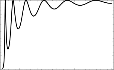
0.8 0.8
0.6 0.6 T T 0.4 0.4
0.2 0.2
0.0 0.0
300 400 500 600 700 800 900 E +meV /
Figure 5.2 Typical T versus E curve of tunnel barrier for V 0 < E < 900 meV i.e. for non-tunneling regime. Barrier width 2a = w = 20 nm, Al content of Al x Ga 1−x As x = 0.4. Using program number 5.1. We find oscillatory variation of transmission coefficient with monotonic variation of amplitude as function of energy E. Looking at Figure 5.2, we find oscillatory variation of transmission coefficient as function of energy E. Amplitude of the oscillations varies monotonically as function of energy E. Key to understanding the oscillations is equation (5.2b): 1
= for E > V 0 ) V , a 2 , E ( T
0 · § 2
¸
+
1 a 2
( )
¸
!
¹ © 0
in which we find that for given values of 2a and V 0 , the oscillations result from
· § −

)
¸ ¨
2
term which oscillates between 0 and 1 as a 2 sin
oscillatory
¸ ¨ !
¹ ©
function of energy E.
Oscillatory transmission through non-tunneling regime of single rectangular tunnel barrier:
Parametric dependence of maxima and of minima
Md Mahmud Hasan and Sujaul Chowdhury
Key to understanding the monotonic variation of amplitude of the oscillations 1
is the fact that T oscillates between 1 and roughly . Maxima of T are
2
V 1
0 + 1 ( )
− V E E 4
0 1
always 1 but minima of T are roughly which rises monotonically as
2
V 1
0 + 1 ( )
− V E E 4
0 function of E, as depicted in Figure 5.3 below obtained using program number 5.2 copied below. This explains why amplitude of oscillations in Figure 5.2 monotonically decreases with increasing value of E.
E +meV / 300 400 500 600 700 800 900
1.0 1.0
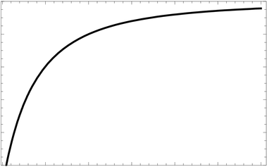
0.8 0.8
0.6 0.6
min min T T
0.4 0.4
0.2 0.2
0.0 0.0
300 400 500 600 700 800 900 E +meV /
1
= Figure 5.3 Figure showing that rises monotonically for T
min
2
V 1
0 + 1 ( )
− V E E 4
0 larger value of E. Using program number 5.2. This explains why amplitude of oscillations in Figure 5.2 monotonically decreases with increasing value of E.
Chapter V Numerical investigation of parametric dependence of transmission through
non-tunneling regime of single rectangular tunnel barrier: Qualitative aspects Program number 5.2 x=0.4
w=20*10^-9
m=0.067*9.1*10^-31
hcut=(6.626*10^-34)/(2*3.1416)
V0=773*x
gamma=Sqrt[2*m*(X-V0)*1.6*10^-22/hcut^2]
Tmin=1/(1+0.25*((V0^2)/(X*(X-V0))))
Plot[Tmin,{X,V0,900},PlotRange->{0,1},Frame->True,
PlotStyle->{Thick,Black},
FrameLabel->{{"T min ","T min "},{"E (meV)","E (meV)"}},FrameTicks->All]
5.3 Dependence of oscillatory transmission coefficient on tunnel barrier height
Using equation (5.2a), we have written program number 5.3 copied below to reveal dependence of oscillatory transmission coefficient on tunnel barrier height. The parametric dependence is shown in Figure 5.4.
Program number 5.3
x1=0.3
x2=0.35
x3=0.4
w=10*10^-9
m=0.067*9.1*10^-31
hcut=(6.626*10^-34)/(2*3.1416)
V01=773*x1
V02=773*x2
V03=773*x3
gamma1=Sqrt[2*m*(X-V01)*1.6*10^-22/hcut^2]
gamma2=Sqrt[2*m*(X-V02)*1.6*10^-22/hcut^2]
gamma3=Sqrt[2*m*(X-V03)*1.6*10^-22/hcut^2]
T1=1/(1+0.25*((V01^2)/(X*(X-V01)))*(Sin[gamma1*w])^2)
T2=1/(1+0.25*((V02^2)/(X*(X-V02)))*(Sin[gamma2*w])^2)
T3=1/(1+0.25*((V03^2)/(X*(X-V03)))*(Sin[gamma3*w])^2)
Oscillatory transmission through non-tunneling regime of single rectangular tunnel barrier:
Parametric dependence of maxima and of minima
Md Mahmud Hasan and Sujaul Chowdhury
p1=Plot[{T1},{X,V01,900},PlotRange->{0,1},Frame->True,
PlotStyle->{{Thick,Dotted,Black}}];
p2=Plot[{T2},{X,V02,900},PlotRange->{0,1},Frame->True,
PlotStyle->{{Thick,Dashed,Black}}];
p3=Plot[{T3},{X,V03,900},PlotRange->{0,1},Frame->True,
PlotStyle->{{Thick,Black}}];
Show[p1,p2,p3,FrameTicks->All,Axes->None,PlotRange->{0,1},
FrameLabel->{{"T","T"},{"E (meV)","E (meV)"}}]
Show[p1,p2,p3,FrameTicks->All,Axes->None,PlotRange->{0.5,1},
FrameLabel->{{"T","T"},{"E (meV)","E (meV)"}}]
E +meV / 300 400 500 600 700 800 900
1.0 1.0
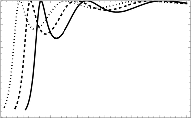
0.8 0.8
0.6 0.6 T T 0.4 0.4
0.2 0.2
0.0 0.0
300 400 500 600 700 800 900 E +meV /
Figure 5.4 T versus E curves of tunnel barrier for V 01 , V 02 , V 03 < E < 900 meV for dotted, dashed and undashed curve respectively for non-tunneling regime. Barrier width 2a = w = 10 nm, Al content of Al x Ga 1−x As x = 0.3 for dotted curve, x = 0.35 for dashed curve and x = 0.4 for undashed curve. Using program number 5.3. The three values of Al content x of Al x Ga 1−x As correspond to three different values of barrier height.
Chapter V Numerical investigation of parametric dependence of transmission through
non-tunneling regime of single rectangular tunnel barrier: Qualitative aspects There are several striking features of the parametric dependence shown in Figure 5.4.
1) Values of energy E for which transmission peaks occur go to higher values of E for larger barrier height.
2) Values of energy E for which transmission minima occur also go to higher values of E for larger barrier height.
3) Values of transmission coefficient T at minima decrease with increasing barrier height. Explanations of the above mentioned three features of the parametric dependences are as follows. According to equation (5.2b): 1
= for E > V 0 ) V , a 2 , E ( T
0 · § 2
¸
+
a 2 1
( )
¸
!
¹ © 0
· § −

)
¸ ¨
=
0 a 2 sin
peaks in T versus E curve obey the condition or,
¸ ¨ !
¹ ©

π =
where n = 1, 2, 3, … . Thus values of energy for which
n a 2
!
2 2 § π ! · n
+ = ¸ ¨ V E which are obviously transmission peaks occur are given by
pn 0
¹ © a 2 m 2 larger for larger values of barrier height V 0 . Again, according to equation (5.2b): 1
= for E > V 0 ) V , a 2 , E ( T
0 · § 2
¸
+
a 2 1
( )
¸
!
¹ ©
· § −

)
¸ ¨
2 = 1 a 2 sin minima in T versus E curve roughly obey the condition
¸ ¨ !
¹ ©
or, where n = 0, 1, 2, 3, … . Thus values of energy
!
Oscillatory transmission through non-tunneling regime of single rectangular tunnel barrier:
Parametric dependence of maxima and of minima
Md Mahmud Hasan and Sujaul Chowdhury
2 2 π ! · §
+ = + ¸ ¨ V ) 1 n 2 ( E for which transmission minima occur are given by
0 mn
¹ © a 4 m 2 which are also obviously larger for larger values of barrier height V 0 . Again, according to equation (5.2b): 1
= for E > V 0 ) V , a 2 , E ( T
0 · § 2
¸
+
a 2 1
( )
¸
!
¹ © 0
values of transmission coefficient T at minima of T versus E curve roughly obey the 1
= condition . It is evident that value of T at minima i.e. T min is T
min
2
V 1
0 + 1 ( ) − V E E 4
0 smaller for larger value of barrier height V 0 . Parametric dependence as in Figure 5.4 can also be found in Figure 5.5 to Figure 5.12, obtained using program number 5.3 above using several chosen values of the two parameters: Al content x of Al x Ga 1−x As (which determines height of the barrier) and barrier width 2a = w. The above-mentioned three features can be observed in all these Figures i.e. in Figure 5.5 to 5.12.
Chapter V Numerical investigation of parametric dependence of transmission through
non-tunneling regime of single rectangular tunnel barrier: Qualitative aspects
E +meV / 200 300 400 500 600 700 800 900
1.0 1.0
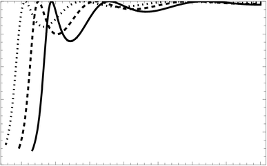
0.8 0.8
0.6 0.6 T T 0.4 0.4
0.2 0.2
0.0 0.0
200 300 400 500 600 700 800 900 E +meV /
Figure 5.5 T versus E curves of tunnel barrier for V 01 , V 02 , V 03 < E < 900 meV for dotted, dashed and undashed curve respectively for non-tunneling regime. Barrier width 2a = w = 10 nm, Al content of Al x Ga 1−x As x = 0.2 for dotted curve, x = 0.25 for dashed curve and x = 0.3 for undashed curve. Using program number 5.3. The three values of Al content x of Al x Ga 1−x As correspond to three different values of barrier height.
Oscillatory transmission through non-tunneling regime of single rectangular tunnel barrier:
Parametric dependence of maxima and of minima
Md Mahmud Hasan and Sujaul Chowdhury
E +meV / 0 200 400 600 800
1.0 1.0
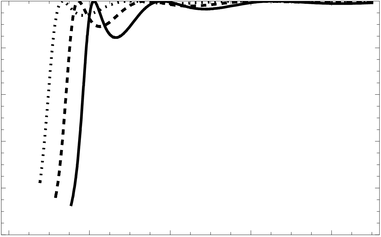
0.8 0.8
0.6 0.6 T T 0.4 0.4
0.2 0.2
0.0 0.0
0 200 400 600 800
E +meV /
Figure 5.6 T versus E curves of tunnel barrier for V 01 , V 02 , V 03 < E < 900 meV for dotted, dashed and undashed curve respectively for non-tunneling regime. Barrier width 2a = w = 10 nm, Al content of Al x Ga 1−x As x = 0.1 for dotted curve, x = 0.15 for dashed curve and x = 0.2 for undashed curve. Using program number 5.3. The three values of Al content x of Al x Ga 1−x As correspond to three different values of barrier height.
Chapter V Numerical investigation of parametric dependence of transmission through
non-tunneling regime of single rectangular tunnel barrier: Qualitative aspects For larger values of barrier width, e.g. 15 or 20 nm, oscillatory curves mingle and it becomes difficult to keep track of which peak or minimum moved where. As such for larger values of barrier widths, we compared curves for smaller increments of Al content of AlGaAs. This is shown in Figure 5.7 to 5.12.
E +meV / 300 400 500 600 700 800 900
1.0 1.0
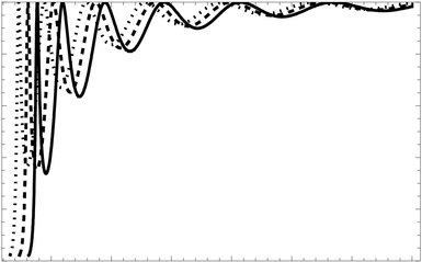
0.8 0.8
0.6 0.6 T T 0.4 0.4
0.2 0.2
0.0 0.0
300 400 500 600 700 800 900 E +meV /
Figure 5.7 T versus E curves of tunnel barrier for V 01 , V 02 , V 03 < E < 900 meV for dotted, dashed and undashed curve respectively for non-tunneling regime. Barrier width 2a = w = 20 nm, Al content of Al x Ga 1−x As x = 0.3 for dotted curve, x = 0.32 for dashed curve and x = 0.34 for undashed curve. Using program number 5.3. The three values of Al content x of Al x Ga 1−x As correspond to three different values of barrier height.
Oscillatory transmission through non-tunneling regime of single rectangular tunnel barrier:
Parametric dependence of maxima and of minima
Md Mahmud Hasan and Sujaul Chowdhury
E +meV / 300 400 500 600 700 800 900
1.0 1.0
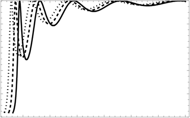
0.8 0.8
0.6 0.6 T T 0.4 0.4
0.2 0.2
0.0 0.0
300 400 500 600 700 800 900
E +meV /
Figure 5.8 T versus E curves of tunnel barrier for V 01 , V 02 , V 03 < E < 900 meV for dotted, dashed and undashed curve respectively for non-tunneling regime. Barrier width 2a = w = 15 nm, Al content of Al x Ga 1−x As x = 0.3 for dotted curve, x = 0.32 for dashed curve and x = 0.34 for undashed curve. Using program number 5.3. The three values of Al content x of Al x Ga 1−x As correspond to three different values of barrier height.
Chapter V Numerical investigation of parametric dependence of transmission through
non-tunneling regime of single rectangular tunnel barrier: Qualitative aspects
E +meV / 200 300 400 500 600 700 800 900
1.0 1.0
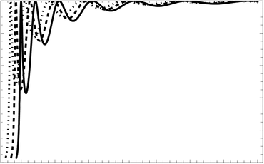
0.8 0.8
0.6 0.6 T T
0.4 0.4
0.2 0.2
0.0 0.0
200 300 400 500 600 700 800 900
E +meV /
Figure 5.9 T versus E curves of tunnel barrier for V 01 , V 02 , V 03 < E < 900 meV for dotted, dashed and undashed curve respectively for non-tunneling regime. Barrier width 2a = w = 20 nm, Al content of Al x Ga 1−x As x = 0.2 for dotted curve, x = 0.22 for dashed curve and x = 0.24 for undashed curve. Using program number 5.3. The three values of Al content x of Al x Ga 1−x As correspond to three different values of barrier height.
Oscillatory transmission through non-tunneling regime of single rectangular tunnel barrier:
Parametric dependence of maxima and of minima
Md Mahmud Hasan and Sujaul Chowdhury
E +meV / 200 300 400 500 600 700 800 900
1.0 1.0
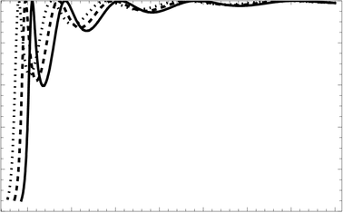
0.8 0.8
0.6 0.6 T T 0.4 0.4
0.2 0.2
0.0 0.0
200 300 400 500 600 700 800 900
E +meV /
Figure 5.10 T versus E curves of tunnel barrier for V 01 , V 02 , V 03 < E < 900 meV for dotted, dashed and undashed curve respectively for non-tunneling regime. Barrier width 2a = w = 15 nm, Al content of Al x Ga 1−x As x = 0.2 for dotted curve, x = 0.22 for dashed curve and x = 0.24 for undashed curve. Using program number 5.3. The three values of Al content x of Al x Ga 1−x As correspond to three different values of barrier height.
Chapter V Numerical investigation of parametric dependence of transmission through
non-tunneling regime of single rectangular tunnel barrier: Qualitative aspects
E +meV / 0 200 400 600 800
1.0 1.0
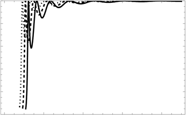
0.8 0.8
0.6 0.6 T T 0.4 0.4
0.2 0.2
0.0 0.0
0 200 400 600 800 E +meV /
Figure 5.11 T versus E curves of tunnel barrier for V 01 , V 02 , V 03 < E < 900 meV for dotted, dashed and undashed curve respectively for non-tunneling regime. Barrier width 2a = w = 20 nm, Al content of Al x Ga 1−x As x = 0.1 for dotted curve, x = 0.12 for dashed curve and x = 0.14 for undashed curve. Using program number 5.3. The three values of Al content x of Al x Ga 1−x As correspond to three different values of barrier height.
Oscillatory transmission through non-tunneling regime of single rectangular tunnel barrier:
Parametric dependence of maxima and of minima
Md Mahmud Hasan and Sujaul Chowdhury
E +meV / 0 200 400 600 800
1.0 1.0
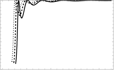
0.8 0.8
0.6 0.6 T T 0.4 0.4
0.2 0.2
0.0 0.0
0 200 400 600 800
E +meV /
Figure 5.12 T versus E curves of tunnel barrier for V 01 , V 02 , V 03 < E < 900 meV for dotted, dashed and undashed curve respectively for non-tunneling regime. Barrier width 2a = w = 15 nm, Al content of Al x Ga 1−x As x = 0.1 for dotted curve, x = 0.12 for dashed curve and x = 0.14 for undashed curve. Using program number 5.3. The three values of Al content x of Al x Ga 1−x As correspond to three different values of barrier height.
Chapter V Numerical investigation of parametric dependence of transmission through
non-tunneling regime of single rectangular tunnel barrier: Qualitative aspects
5.4 Dependence of oscillatory transmission coefficient on tunnel barrier width
Using equation (5.2a), we have written program number 5.4 copied below to reveal dependence of oscillatory transmission coefficient on barrier width. The parametric dependence is shown in Figure 5.13 below. E +meV / 300 400 500 600 700 800 900
1.0 1.0
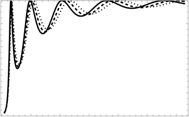
0.8 0.8
0.6 0.6 T T 0.4 0.4
0.2 0.2
0.0 0.0
300 400 500 600 700 800 900 E +meV /
Figure 5.13 T versus E curves of tunnel barrier for V 0 < E < 3V 0 for non-tunneling regime. For barrier width 2a = w = 15 nm (dotted curve), 15.5 nm (dashed curve) and 16 nm (undashed curve) and Al content of Al x Ga 1−x As x = 0.4. Using program number 5.4.
Program number 5.4
x=0.4
w1=15*10^-9
w2=15.5*10^-9
w3=16*10^-9
m=0.067*9.1*10^-31
hcut=(6.626*10^-34)/(2*3.1416)
V0=773*x
gamma=Sqrt[2*m*(X-V0)*1.6*10^-22/hcut^2]
Oscillatory transmission through non-tunneling regime of single rectangular tunnel barrier:
Parametric dependence of maxima and of minima
Md Mahmud Hasan and Sujaul Chowdhury
T1=1/(1+0.25*((V0^2)/(X*(X-V0)))*(Sin[gamma*w1])^2)
T2=1/(1+0.25*((V0^2)/(X*(X-V0)))*(Sin[gamma*w2])^2)
T3=1/(1+0.25*((V0^2)/(X*(X-V0)))*(Sin[gamma*w3])^2)
Plot[{T1,T2,T3},{X,V0,3*V0},PlotRange->{0,1},Frame->True,
PlotStyle->{{Thick,Dotted,Black},{Thick,Dashed,Black},{Thick,Black}},
FrameLabel->{{"T","T"},{"E (meV)","E (meV)"}},FrameTicks->All]
Plot[{T1,T2,T3},{X,V0,3*V0},PlotRange->{0.5,1},Frame->True,
PlotStyle->{{Thick,Dotted,Black},{Thick,Dashed,Black},{Thick,Black}},
FrameLabel->{{"T","T"},{"E (meV)","E (meV)"}},FrameTicks->All]
In obtaining the parametric dependence shown in Figure 5.13, we have deliberately chosen three close values of barrier width 2a or w, namely 15, 15.5 and 16 nm. This is because, for more widely spaced values of 2a, it is difficult or even impossible to keep track of which peak moved where and which minima moved where. There are several striking features of the parametric dependence shown in Figure 5.13.
1) Values of energy E for which transmission peaks occur go to lower energy E for larger barrier width.
2) Values of energy E for which transmission minima occur go to lower energy E for larger barrier width.
3) Values of transmission coefficient T at minima decrease with increasing barrier width. Explanations of the above mentioned three features of the parametric dependences are as follows. According to equation (5.2b): 1
= for E > V 0 ) V , a 2 , E ( T
0 · § 2

¸
+
a 2 1
( )
¸
!
¹ © 0
Chapter V Numerical investigation of parametric dependence of transmission through
non-tunneling regime of single rectangular tunnel barrier: Qualitative aspects
· § −

)
¸ ¨
2 = 0 a 2 sin peaks in T versus E curve obey the condition or,
¸ ¨ !
¹ ©

π =
where n = 1, 2, 3, … . Thus values of energy for which
n a 2
!
2 2 § π ! · n
= + ¸ ¨ V E transmission peaks occur are given by which are obviously
0 pn
¹ © a 2 m 2 lower for larger barrier width 2a or w in inverse square fashion. Again, according to equation (5.2b): 1
= for E > V 0 ) V , a 2 , E ( T
0 · § 2
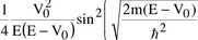
¸
+
a 2 1
( )
¸
!
¹ © 0
· § −

)
¸ ¨
2 = 1 a 2 sin minima in T versus E curve roughly obey the condition
¸ ¨ !
¹ ©
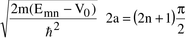
or, where n = 0, 1, 2, 3, … . Thus values of energy
!
2 2 π ! · §
+ = + ¸ ¨ V ) 1 n 2 ( E for which transmission minima occur are given by
0 mn
¹ © a 4 m 2 which are also lower for larger barrier width 2a or w in inverse square fashion. Again, according to equation (5.2b): 1
= for E > V 0 ) V , a 2 , E ( T
0 · § 2
¸
+
a 2 1
( )
¸
!
¹ © 0
values of transmission coefficient T at minima of T versus E curve roughly obey the 1
= condition . It may seem that T min is independent of barrier T
min
2
V 1
0 + 1 ( ) − V E E 4
0 width 2a or w. But we need to note here that values of E for minima become lower
Oscillatory transmission through non-tunneling regime of single rectangular tunnel barrier:
Parametric dependence of maxima and of minima
Md Mahmud Hasan and Sujaul Chowdhury
1
= for larger 2a or w. Use of this lower value of E in shows that T
min
2
V 1
0 + 1 ( ) − V E E 4
0 T is lower at minima for larger barrier width 2a or w. Parametric dependence as in Figure 5.13 can also be found in Figure 5.14 to Figure 5.24, obtained using program number 5.4 above using several chosen values of the two parameters: Al content x of Al x Ga 1−x As (which determines height of the barrier) and barrier width 2a or w.
E +meV / 300 400 500 600 700
1.0 1.0
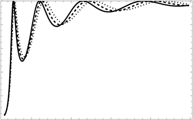
0.8 0.8
0.6 0.6 T T 0.4 0.4
0.2 0.2
0.0 0.0
300 400 500 600 700
E +meV /
Figure 5.14 T versus E curves of tunnel barrier for V 0 < E < 3V 0 for non-tunneling regime. For barrier width 2a = w = 15 nm (dotted curve), 15.5 nm (dashed curve) and 16 nm (undashed curve) and Al content of Al x Ga 1−x As x = 0.3. Using program number 5.4.
Chapter V Numerical investigation of parametric dependence of transmission through
non-tunneling regime of single rectangular tunnel barrier: Qualitative aspects
E +meV / 150 200 250 300 350 400 450
1.0 1.0
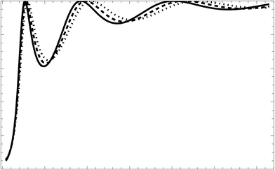
0.8 0.8
0.6 0.6 T T 0.4 0.4
0.2 0.2
0.0 0.0
150 200 250 300 350 400 450
E +meV /
Figure 5.15 T versus E curves of tunnel barrier for V 0 < E < 3V 0 for non-tunneling regime. For barrier width 2a = w = 15 nm (dotted curve), 15.5 nm (dashed curve) and 16 nm (undashed curve) and Al content of Al x Ga 1−x As x = 0.2. Using program number 5.4.
Oscillatory transmission through non-tunneling regime of single rectangular tunnel barrier:
Parametric dependence of maxima and of minima
Md Mahmud Hasan and Sujaul Chowdhury
E +meV /
100 150 200
1.0 1.0
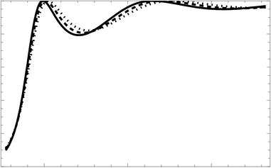
0.8 0.8
0.6 0.6 T T 0.4 0.4
0.2 0.2
0.0 0.0
100 150 200 E +meV /
Figure 5.16 T versus E curves of tunnel barrier for V 0 < E < 3V 0 for non-tunneling regime. For barrier width 2a = w = 15 nm (dotted curve), 15.5 nm (dashed curve) and 16 nm (undashed curve) and Al content of Al x Ga 1−x As x = 0.1. Using program number 5.4.
Chapter V Numerical investigation of parametric dependence of transmission through
non-tunneling regime of single rectangular tunnel barrier: Qualitative aspects
E +meV / 300 400 500 600 700 800 900
1.0 1.0
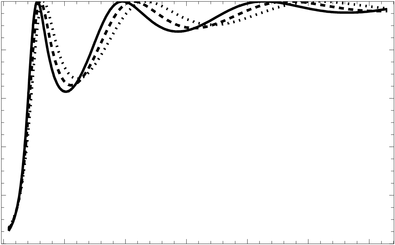
0.8 0.8
0.6 0.6 T T 0.4 0.4
0.2 0.2
0.0 0.0
300 400 500 600 700 800 900
E +meV / Figure 5.17 T versus E curves of tunnel barrier for V 0 < E < 3V 0 for non-tunneling regime. For barrier width 2a = w = 10 nm (dotted curve), 10.5 nm (dashed curve) and 11 nm (undashed curve) and Al content of Al x Ga 1−x As x = 0.4. Using program number 5.4.
Oscillatory transmission through non-tunneling regime of single rectangular tunnel barrier:
Parametric dependence of maxima and of minima
Md Mahmud Hasan and Sujaul Chowdhury
E +meV / 300 400 500 600 700
1.0 1.0
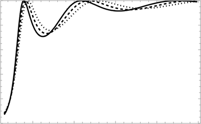
0.8 0.8
0.6 0.6 T T 0.4 0.4
0.2 0.2
0.0 0.0
300 400 500 600 700
E +meV /
Figure 5.18 T versus E curves of tunnel barrier for V 0 < E < 3V 0 for non-tunneling regime. For barrier width 2a = w = 10 nm (dotted curve), 10.5 nm (dashed curve) and 11 nm (undashed curve) and Al content of Al x Ga 1−x As x = 0.3. Using program number 5.4.
Chapter V Numerical investigation of parametric dependence of transmission through
non-tunneling regime of single rectangular tunnel barrier: Qualitative aspects
E +meV / 150 200 250 300 350 400 450
1.0 1.0
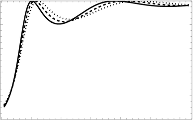
0.8 0.8
0.6 0.6 T T 0.4 0.4
0.2 0.2
0.0 0.0
150 200 250 300 350 400 450
E +meV /
Figure 5.19 T versus E curves of tunnel barrier for V 0 < E < 3V 0 for non-tunneling regime. For barrier width 2a = w = 10 nm (dotted curve), 10.5 nm (dashed curve) and 11 nm (undashed curve) and Al content of Al x Ga 1−x As x = 0.2. Using program number 5.4.
Oscillatory transmission through non-tunneling regime of single rectangular tunnel barrier:
Parametric dependence of maxima and of minima
Md Mahmud Hasan and Sujaul Chowdhury
E +meV / 100 150 200
1.0 1.0
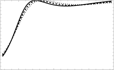
0.8 0.8
0.6 0.6 T T 0.4 0.4
0.2 0.2
0.0 0.0
100 150 200 E +meV /
Figure 5.20 T versus E curves of tunnel barrier for V 0 < E < 3V 0 for non-tunneling regime. For barrier width 2a = w = 10 nm (dotted curve), 10.5 nm (dashed curve) and 11 nm (undashed curve) and Al content of Al x Ga 1−x As x = 0.1. Using program number 5.4.
Chapter V Numerical investigation of parametric dependence of transmission through
non-tunneling regime of single rectangular tunnel barrier: Qualitative aspects
E +meV / 300 400 500 600 700 800 900
1.0 1.0
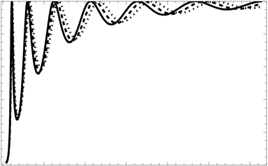
0.8 0.8
0.6 0.6 T T 0.4 0.4
0.2 0.2
0.0 0.0
300 400 500 600 700 800 900 E +meV /
Figure 5.21 T versus E curves of tunnel barrier for V 0 < E < 3V 0 for non-tunneling regime. For barrier width 2a = w = 20 nm (dotted curve), 20.5 nm (dashed curve) and 21 nm (undashed curve) and Al content of Al x Ga 1−x As x = 0.4. Using program number 5.4.
Oscillatory transmission through non-tunneling regime of single rectangular tunnel barrier:
Parametric dependence of maxima and of minima
Md Mahmud Hasan and Sujaul Chowdhury
E +meV / 300 400 500 600 700
1.0 1.0
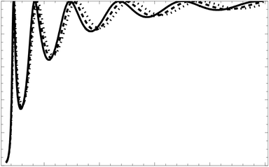
0.8 0.8
0.6 0.6 T T 0.4 0.4
0.2 0.2
0.0 0.0
300 400 500 600 700 E +meV /
Figure 5.22 T versus E curves of tunnel barrier for V 0 < E < 3V 0 for non-tunneling regime. For barrier width 2a = w = 20 nm (dotted curve), 20.5 nm (dashed curve) and 21 nm (undashed curve) and Al content of Al x Ga 1−x As x = 0.3. Using program number 5.4.
Chapter V Numerical investigation of parametric dependence of transmission through
non-tunneling regime of single rectangular tunnel barrier: Qualitative aspects
E +meV / 150 200 250 300 350 400 450
1.0 1.0
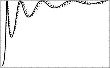
0.8 0.8
0.6 0.6 T T 0.4 0.4
0.2 0.2
0.0 0.0
150 200 250 300 350 400 450 E +meV /
Figure 5.23 T versus E curves of tunnel barrier for V 0 < E < 3V 0 for non-tunneling regime. For barrier width 2a = w = 20 nm (dotted curve), 20.5 nm (dashed curve) and 21 nm (undashed curve) and Al content of Al x Ga 1−x As x = 0.2. Using program number 5.4.
Oscillatory transmission through non-tunneling regime of single rectangular tunnel barrier:
Parametric dependence of maxima and of minima
Md Mahmud Hasan and Sujaul Chowdhury
E +meV / 100 150 200
1.0 1.0
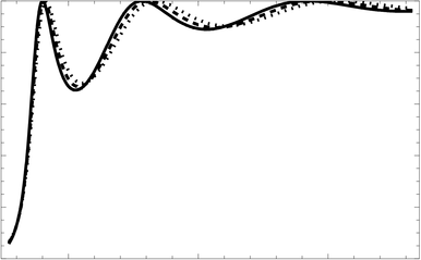
0.8 0.8
0.6 0.6 T T 0.4 0.4
0.2 0.2
0.0 0.0
100 150 200 E +meV /
Figure 5.24 T versus E curves of tunnel barrier for V 0 < E < 3V 0 for non-tunneling regime. For barrier width 2a = w = 20 nm (dotted curve), 20.5 nm (dashed curve) and 21 nm (undashed curve) and Al content of Al x Ga 1−x As x = 0.1. Using program number 5.4.
Oscillatory transmission through non-tunneling regime of single rectangular tunnel barrier:
Parametric dependence of maxima and of minima
Md Mahmud Hasan and Sujaul Chowdhury
Quantitative aspects
Chapter VI: Numerical investigation of parametric dependence of transmission peaks
for non-tunneling regime of single rectangular tunnel barrier: Quantitative aspects
6.1 The analytical expressions for transmission coefficient of single rectangular tunnel barrier for non-tunneling regime
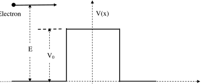
Electron
− a (0, 0) + a x Figure 6.1 A single rectangular tunnel barrier being traversed by an electron in nontunneling regime. We repeat the following of this section for ready reference. Figure 6.1 shows a single rectangular tunnel barrier of width 2a and height V 0 being traversed by an electron of total energy E > V 0 . Tunnel barrier was introduced in section 3.1.1 and 3.1.2. Width 2a of the barrier is nano-scale, e.g. 10 nm and height V 0 is typically 300 meV. V 0 is conduction band offset between QW material (e.g. GaAs) and barrier material (e.g. Al x Ga 1−x As). x is Al content of AlGaAs that determines the conduction band offset usually taken as V 0 = ΔE c = 773x meV.
Referring to the potential profile in Figure 6.1, the necessary analytical expressions for transmission coefficient T of the barrier as function of total energy E of electron for non-tunneling regime were derived in Chapter IV and are given by equation (4.24) or (4.25). Here we gather the expressions for ready reference. 1
= for E > V 0 ---------(6.1) T
γ k 1 2 2 γ − + a 2 sin ) ( 1
γ 4 k 1
= for E > V 0 ---------(6.2a) ) V , a 2 , E ( T
0
2
V 1 2 0 γ + a 2 sin 1 ( )
− V E E 4
0
Oscillatory transmission through non-tunneling regime of single rectangular tunnel barrier:
Parametric dependence of maxima and of minima
Md Mahmud Hasan and Sujaul Chowdhury
1
= for E > V 0 --------(6.2b) ) V , a 2 , E ( T
0 · § 2
¸
+
a 2 1
( )
¸
!
¹ © 0 − ) V E ( m 2 mE 2 2 2 0 = γ = k Here , , 2a is width and V 0 is height of the barrier.
2 2 ! ! Equation (6.1) or (6.2a) or (6.2b) is the expression for transmission coefficient T of electron across non-tunneling regime, i.e. for E > V 0 , of tunnel barrier. E is total energy i.e. kinetic plus potential energy of electron. Outside the barrier region, E is kinetic energy as well as total energy because potential energy is zero outside the barrier region by choice of origin. In this chapter, we have investigated parametric dependences of energy of transmission peaks for non-tunneling regime of tunnel barrier. We have put the condition obeyed by the transmission peaks in the form of a program written in Mathematica 6.0 and have quantitatively investigated parametric dependences of energy of transmission peaks. We have also completely explained the parametric dependences both qualitatively and quantitatively.
6.2 Parametric dependences of transmission peaks: quantitative account
According to equation (6.2b), transmission peaks obey the condition
· § −
¨
π =
sin
where n = 1, 2, 3, … .
n a 2
¨
!
!
¹ ©
Thus values of energy for which transmission peaks occur are given by 2 2 § π ! · n
+ = ¸ ¨ V E . We have written this condition in the form of program
pn 0
¹ © a 2 m 2 number 6.1 below to obtain values of E p1 , E p2 , E p3 , … in the range V 0 to 900 meV for various values of the two parameters: barrier width 2a = w and Al content x of Al x Ga 1−x As (that determines barrier height V 0 = 773x meV).
Chapter VI: Numerical investigation of parametric dependence of transmission peaks
for non-tunneling regime of single rectangular tunnel barrier: Quantitative aspects Program number 6.1 n1=1
n2=2
n3=3
n4=4
n5=5
n6=6
n7=7
n8=8
n9=9
n10=10
n11=11
n12=12
x=0.4
w=20*10^-9
m=0.067*9.1*10^-31
hcut=(6.626*10^-34)/(2*3.1416)
V0=773*x
gamma=Sqrt[2*m*(X-V0)*1.6*10^-22/hcut^2]
T=1/(1+0.25*((V0^2)/(X*(X-V0)))*(Sin[gamma*w])^2)
Plot[T,{X,V0,900},PlotRange->{0,1},Frame->True,PlotStyle->{Thick,Black},
FrameLabel->{{"T","T"},{"E (meV)","E (meV)"}},FrameTicks->All,Axes->None]
Plot[T,{X,V0,900},PlotRange->{0.5,1},Frame->True,PlotStyle->{Thick,Black},
FrameLabel->{{"T","T"},{"E (meV)","E (meV)"}},FrameTicks->All,Axes->None]
V0=773*x
Ep1=(n1^2)*(((hcut^2)/(2*m))*((3.1416/w)^2))/(1.6*10^-22)+V0
Ep2=(n2^2)*(((hcut^2)/(2*m))*((3.1416/w)^2))/(1.6*10^-22)+V0
Ep3=(n3^2)*(((hcut^2)/(2*m))*((3.1416/w)^2))/(1.6*10^-22)+V0
Ep4=(n4^2)*(((hcut^2)/(2*m))*((3.1416/w)^2))/(1.6*10^-22)+V0
Ep5=(n5^2)*(((hcut^2)/(2*m))*((3.1416/w)^2))/(1.6*10^-22)+V0
Ep6=(n6^2)*(((hcut^2)/(2*m))*((3.1416/w)^2))/(1.6*10^-22)+V0
Ep7=(n7^2)*(((hcut^2)/(2*m))*((3.1416/w)^2))/(1.6*10^-22)+V0
Ep8=(n8^2)*(((hcut^2)/(2*m))*((3.1416/w)^2))/(1.6*10^-22)+V0
Ep9=(n9^2)*(((hcut^2)/(2*m))*((3.1416/w)^2))/(1.6*10^-22)+V0
Ep10=(n10^2)*(((hcut^2)/(2*m))*((3.1416/w)^2))/(1.6*10^-22)+V0
Ep11=(n11^2)*(((hcut^2)/(2*m))*((3.1416/w)^2))/(1.6*10^-22)+V0
Ep12=(n12^2)*(((hcut^2)/(2*m))*((3.1416/w)^2))/(1.6*10^-22)+V0
Oscillatory transmission through non-tunneling regime of single rectangular tunnel barrier:
Parametric dependence of maxima and of minima
Md Mahmud Hasan and Sujaul Chowdhury
Table 6.1 For x = 0.1 and w =2a = 20 nm, we obtain E pn ’s in meV:

Table 6.2 For x = 0.1 and w = 2a = 15 nm, we obtain E pn ’s in meV:

Table 6.3 For x = 0.1 and w = 2a = 10 nm, we obtain E pn ’s in meV:

Table 6.4 For x = 0.1 and w = 2a = 5 nm, we obtain E pn ’s in meV:
Chapter VI: Numerical investigation of parametric dependence of transmission peaks
for non-tunneling regime of single rectangular tunnel barrier: Quantitative aspects
Table 6.5 For x = 0.2 and w = 2a = 20 nm, we obtain E pn ’s in meV:

Table 6.6 For x = 0.2 and w = 2a = 15 nm, we obtain E pn ’s in meV:

Table 6.7 For x = 0.2 and w = 2a = 10 nm, we obtain E pn ’s in meV:

Table 6.8 For x = 0.2 and w = 2a = 5 nm, we obtain E pn ’s in meV:

Oscillatory transmission through non-tunneling regime of single rectangular tunnel barrier:
Parametric dependence of maxima and of minima
Md Mahmud Hasan and Sujaul Chowdhury
Table 6.9 For x = 0.3 and w = 2a = 20 nm, we obtain E pn ’s in meV:

Table 6.10 For x = 0.3 and w = 2a = 15 nm, we obtain E pn ’s in meV:

Table 6.11 For x = 0.3 and w = 2a = 10 nm, we obtain E pn ’s in meV:

Table 6.12 For x = 0.3 and w = 2a = 5 nm, we obtain E pn ’s in meV:

Chapter VI: Numerical investigation of parametric dependence of transmission peaks
for non-tunneling regime of single rectangular tunnel barrier: Quantitative aspects
Table 6.13 For x = 0.4 and w = 2a = 20 nm, we obtain E pn ’s in meV:

Table 6.14 For x = 0.4 and w = 2a = 15 nm, we obtain E pn ’s in meV:

Table 6.15 For x = 0.4 and w = 2a = 10 nm, we obtain E pn ’s in meV:

Table 6.16 For x = 0.4 and w = 2a = 5 nm, we obtain E pn ’s in meV:

Oscillatory transmission through non-tunneling regime of single rectangular tunnel barrier:
Parametric dependence of maxima and of minima
Md Mahmud Hasan and Sujaul Chowdhury
We have re-tabulated the raw data of Table 6.1 to 6.16 above as table 6.17 to 6.24 below to reveal parametric dependences of energy of transmission peaks. Each new table is accompanied with a Figure that provides visual display of the parametric dependence.
Table 6.17

x = 0.4, V 0 = 309 meV 2a (nm)
5 1 0 1 5 2 0
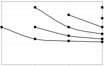
900 900 800 800 700 700 600 600
(meV) (meV)
500 500 E pn 400 400 E pn 300 300 200 200 100 100 0 0
5 1 0 1 5 2 0
2a (nm)
Figure 6.2 Figure showing dependence of energy of transmission peaks on barrier width 2a. For Al content x = 0.4 of Al x Ga 1−x As that correspond to barrier height of 309 meV.
Chapter VI: Numerical investigation of parametric dependence of transmission peaks
for non-tunneling regime of single rectangular tunnel barrier: Quantitative aspects
Table 6.18
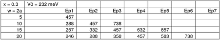
x = 0.3, V 0 = 232 meV 2a (nm)
5 1 0 1 5 2 0
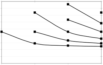
900 900 800 800 700 700 600 600
(meV) (meV)
500 500 E pn 400 400 E pn 300 300 200 200 100 100 0 0
5 1 0 1 5 2 0
2a (nm)
Figure 6.3 Figure showing dependence of energy of transmission peaks on barrier width 2a. For Al content x = 0.3 of Al x Ga 1−x As that correspond to barrier height of 232 meV.
Oscillatory transmission through non-tunneling regime of single rectangular tunnel barrier:
Parametric dependence of maxima and of minima
Md Mahmud Hasan and Sujaul Chowdhury
Figure 6.19

x = 0.2, V 0 = 155 meV 2a (nm)
5 1 0 1 5 2 0
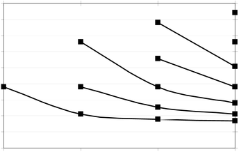
900 900 800 800 700 700 600 600
(meV) (meV)
500 500 E pn 400 400 E pn 300 300 200 200 100 100 0 0
5 1 0 1 5 2 0
2a (nm)
Figure 6.4 Figure showing dependence of energy of transmission peaks on barrier width 2a. For Al content x = 0.2 of Al x Ga 1−x As that correspond to barrier height of 155 meV.
Chapter VI: Numerical investigation of parametric dependence of transmission peaks
for non-tunneling regime of single rectangular tunnel barrier: Quantitative aspects
Table 6.20

x = 0.1, V 0 = 77 meV 2a (nm)
5 1 0 1 5 2 0
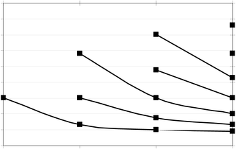
900 900 800 800 700 700 600 600
(meV) (meV)
500 500 E pn 400 400 E pn 300 300 200 200 100 100 0 0
5 1 0 1 5 2 0
2a (nm)
Figure 6.5 Figure showing dependence of energy of transmission peaks on barrier width 2a. For Al content x = 0.1 of Al x Ga 1−x As that correspond to barrier height of 77 meV.
As Figure 6.2 to Figure 6.5 show, energy E pn of transmission peaks decrease with increasing barrier width 2a in inverse square fashion. This we already explained in section 5.4.
Oscillatory transmission through non-tunneling regime of single rectangular tunnel barrier:
Parametric dependence of maxima and of minima
Md Mahmud Hasan and Sujaul Chowdhury
Table 6.21

w = 2a = 20 nm
V 0 (meV)
77 127 177 227 277
900 900 800 800 700 700 600 600
(meV) (meV)
500 500 E pn 400 400 E pn 300 300 200 200 100 100 0 0
0 . 1 0 . 2 0 . 3 0 . 4
x
Figure 6.6 Figure showing dependence of energy of transmission peaks on increasing Al content x of Al x Ga 1−x As that correspond to increasing barrier height V 0 . For barrier width 2a = 20 nm.
Chapter VI: Numerical investigation of parametric dependence of transmission peaks
for non-tunneling regime of single rectangular tunnel barrier: Quantitative aspects
Table 6.22

w = 2a = 15 nm
V 0 (meV)
77 127 177 227 277
900 900 800 800 700 700 600 600
(meV) (meV)
500 500 E pn 400 400 E pn 300 300 200 200 100 100 0 0
0 . 1 0 . 2 0 . 3 0 . 4
x
Figure 6.7 Figure showing dependence of energy of transmission peaks on increasing Al content x of Al x Ga 1−x As that correspond to increasing barrier height V 0 . For barrier width 2a = 15 nm.
Oscillatory transmission through non-tunneling regime of single rectangular tunnel barrier:
Parametric dependence of maxima and of minima
Md Mahmud Hasan and Sujaul Chowdhury
Table 6.23

w = 2a = 10 nm
V 0 (meV)
77 127 177 227 277
900 900 800 800 700 700 600 600
(meV) (meV)
500 500 E pn 400 400 E pn 300 300 200 200 100 100 0 0
0 . 1 0 . 2 0 . 3 0 . 4
x
Figure 6.8 Figure showing dependence of energy of transmission peaks on increasing Al content x of Al x Ga 1−x As that correspond to increasing barrier height V 0 . For barrier width 2a = 10 nm.
Chapter VI: Numerical investigation of parametric dependence of transmission peaks
for non-tunneling regime of single rectangular tunnel barrier: Quantitative aspects
Table 6.24

w = 2a = 5 nm
V 0 (meV)
77 127 177 227 277
900 900 800 800 700 700 600 600
(meV) (meV)
500 500 E pn 400 400 E pn 300 300 200 200 100 100 0 0
0 . 1 0 . 2 0 . 3 0 . 4
x
Figure 6.9 Figure showing dependence of energy of transmission peaks on increasing Al content x of Al x Ga 1−x As that correspond to increasing barrier height V 0 . For barrier width 2a = 5 nm.
As Figure 6.6 to Figure 6.9 show, energy E pn of transmission peaks rises linearly with increasing Al content x of Al x Ga 1−x As that corresponds to increasing barrier height. This we already explained in section 5.3.
Oscillatory transmission through non-tunneling regime of single rectangular tunnel barrier:
Parametric dependence of maxima and of minima
Md Mahmud Hasan and Sujaul Chowdhury
Quantitative aspects
Chapter VII: Numerical investigation of parametric dependence of transmission minima
for non-tunneling regime of single rectangular tunnel barrier: Quantitative aspects
7.1 The analytical expressions for transmission coefficient of single rectangular tunnel barrier for non-tunneling regime
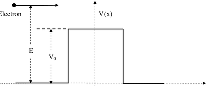
Electron
− a (0, 0) +a x Figure 7.1 An isolated QW being traversed by an electron in non-tunneling regime.
We repeat the following of this section for ready reference. Figure 7.1 shows a single rectangular tunnel barrier of width 2a and height V 0 being traversed by an electron of total energy E > V 0 . The barrier was introduced in section 3.1.1 and 3.1.2. Width 2a of the barrier is nano-scale, e.g. 10 nm and height V 0 is typically 300 meV. V 0 is conduction band offset between QW material (e.g. GaAs) and barrier material (e.g. Al x Ga 1−x As). x is Al content of AlGaAs that determines the conduction band offset usually taken as V 0 = ΔE c = 773x meV. We have calculated in Chapter IV
transfer matrix and transmission coefficient of the barrier for an electron in non- regime. This is a 1D problem. Referring to the potential profile in Figure 7.1, the necessary analytical expressions for transmission coefficient T of the barrier as function of total energy E of electron for non-tunneling regime were derived in Chapter IV and are given by equation (4.24) or (4.25). Here we gather the expressions for ready reference. 1
= for E > V 0 ---------(7.1) T
γ k 1 2 2 γ − + a 2 sin ) ( 1
γ 4 k
Oscillatory transmission through non-tunneling regime of single rectangular tunnel barrier:
Parametric dependence of maxima and of minima
Md Mahmud Hasan and Sujaul Chowdhury
1
= for E > V 0 ---------(7.2a) ) V , a 2 , E ( T
0
2
V 1 2 0 γ + a 2 sin 1 ( )
− V E E 4
0 1
= for E > V 0 --------(7.2b) ) V , a 2 , E ( T
0 § · 2
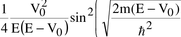
¸
+
1 a 2
( )
¸
!
© ¹ 0 − ) V E ( m 2 mE 2 2 2 0 = = γ k Here , , 2a is width and V 0 is height of the barrier.
2 2 ! ! Equation (7.1) or (7.2a) or (7.2b) is the expression for transmission coefficient T of electron for non-tunneling regime, i.e. for E > V 0 , of single rectangular tunnel barrier. E is total energy i.e. kinetic plus potential energy of electron. Outside the barrier region, E is kinetic energy as well as total energy because potential energy is zero outside the barrier region by choice of origin. In this chapter, we have investigated parametric dependences of energy of transmission minima for non-tunneling regime of single rectangular tunnel barrier. We have put the condition obeyed by transmission minima in the form of a program written in Mathematica 6.0 and have quantitatively investigated parametric dependences of energy of transmission minima. We have also completely explained the parametric dependences both qualitatively and quantitatively.
7.2 Parametric dependences of transmission minima: quantitative account
According to equation (7.2b), transmission minima roughly obey the condition
· § −
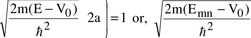
−
¨
( )
2
2
π + =
sin
where n = 0, 1,
/ 1 n 2 a 2
¨
!
!
¹ ©
2, 3, … . Thus values of energy E for which transmission minima occur are given by 2 2 § π ! · ( ) 2 + + = ¸ ¨ V 1 n 2 E . We have written this condition in the form of
mn 0
¹ © a 4 m 2 program number 7.1 below to obtain values of E m1 , E m2 , E m3 , … in the range V 0 to
Chapter VII: Numerical investigation of parametric dependence of transmission minima
for non-tunneling regime of single rectangular tunnel barrier: Quantitative aspects 900 meV for various values of the two parameters: barrier width w = 2a and Al content x of Al x Ga 1−x As (that determines barrier height V 0 = 773x meV).
Program number 7.1 n1=1
n2=2
n3=3
n4=4
n5=5
n6=6
n7=7
n8=8
n9=9
n10=10
n11=11
x=0.4
w=10*10^-9
m=0.067*9.1*10^-31
hcut=(6.626*10^-34)/(2*3.1416)
V0=773*x
gamma=Sqrt[2*m*(X-V0)*1.6*10^-22/hcut^2]
T=1/(1+0.25*((V0^2)/(X*(X-V0)))*(Sin[gamma*w])^2)
Plot[T,{X,V0,900},PlotRange->{0,1},Frame->True,PlotStyle->{Thick,Black},
FrameLabel->{{"T","T"},{"E (meV)","E (meV)"}},FrameTicks->All,Axes->None]
Plot[T,{X,V0,900},PlotRange->{0.5,1},Frame->True,PlotStyle->{Thick,Black},
FrameLabel->{{"T","T"},{"E (meV)","E (meV)"}},FrameTicks->All,Axes->None]
V0=773*x
Em1=((2*n1+1)^2)*(((hcut^2)/(2*m))*((3.1416/(2*w))^2))/(1.6*10^-22)+V0
Em2=((2*n2+1)^2)*(((hcut^2)/(2*m))*((3.1416/(2*w))^2))/(1.6*10^-22)+V0
Em3=((2*n3+1)^2)*(((hcut^2)/(2*m))*((3.1416/(2*w))^2))/(1.6*10^-22)+V0
Em4=((2*n4+1)^2)*(((hcut^2)/(2*m))*((3.1416/(2*w))^2))/(1.6*10^-22)+V0
Em5=((2*n5+1)^2)*(((hcut^2)/(2*m))*((3.1416/(2*w))^2))/(1.6*10^-22)+V0
Em6=((2*n6+1)^2)*(((hcut^2)/(2*m))*((3.1416/(2*w))^2))/(1.6*10^-22)+V0
Em7=((2*n7+1)^2)*(((hcut^2)/(2*m))*((3.1416/(2*w))^2))/(1.6*10^-22)+V0
Em8=((2*n8+1)^2)*(((hcut^2)/(2*m))*((3.1416/(2*w))^2))/(1.6*10^-22)+V0
Em9=((2*n9+1)^2)*(((hcut^2)/(2*m))*((3.1416/(2*w))^2))/(1.6*10^-22)+V0
Em10=((2*n10+1)^2)*(((hcut^2)/(2*m))*((3.1416/(2*w))^2))/(1.6*10^-22)+V0
Em11=((2*n11+1)^2)*(((hcut^2)/(2*m))*((3.1416/(2*w))^2))/(1.6*10^-22)+V0
Oscillatory transmission through non-tunneling regime of single rectangular tunnel barrier:
Parametric dependence of maxima and of minima
Md Mahmud Hasan and Sujaul Chowdhury
Table 7.1 For x = 0.1 and w = 2a = 20 nm, we obtain E mn ’s in meV:

Table 7.2 For x = 0.1 and w = 2a = 15 nm, we obtain E mn ’s in meV:

Table 7.3 For x = 0.1 and w = 2a = 10 nm, we obtain E mn ’s in meV:

Table 7.4 For x = 0.1 and w = 2a = 5 nm, we obtain E mn ’s in meV:

Chapter VII: Numerical investigation of parametric dependence of transmission minima
for non-tunneling regime of single rectangular tunnel barrier: Quantitative aspects
Table 7.5 For x = 0.2 and w = 2a = 20 nm, we obtain E mn ’s in meV:

Table 7.6 For x = 0.2 and w = 2a = 15 nm, we obtain E mn ’s in meV:

Table 7.7 For x = 0.2 and w = 2a = 10 nm, we obtain E mn ’s in meV:

Table 7.8 For x = 0.2 and w = 2a = 5 nm, we obtain E mn ’s in meV:

Oscillatory transmission through non-tunneling regime of single rectangular tunnel barrier:
Parametric dependence of maxima and of minima
Md Mahmud Hasan and Sujaul Chowdhury
Table 7.9 For x = 0.3 and w = 2a = 20 nm, we obtain E mn ’s in meV:

Table 7.10 For x = 0.3 and w = 2a = 15 nm, we obtain E mn ’s in meV:

Table 7.11 For x = 0.3 and w = 2a = 10 nm, we obtain E mn ’s in meV:

Table 7.12 For x = 0.3 and w = 2a = 5 nm, we obtain E mn ’s in meV:

Chapter VII: Numerical investigation of parametric dependence of transmission minima
for non-tunneling regime of single rectangular tunnel barrier: Quantitative aspects
Table 7.13 For x = 0.4 and w = 2a = 20 nm, we obtain E mn ’s in meV:

Table 7.14 For x = 0.4 and w = 2a = 15 nm, we obtain E mn ’s in meV:

Table 7.15 For x = 0.4 and w = 2a = 10 nm, we obtain E mn ’s in meV:

Table 7.16 For x = 0.4 and w = 2a = 5 nm, we obtain E mn ’s in meV:

We have re-tabulated the raw data of Table 7.1 to 7.16 above as table 7.17 to 7.24 below to reveal parametric dependences of energy of transmission minima. Each new table is accompanied with a Figure that provides visual display of the parametric dependence.
Oscillatory transmission through non-tunneling regime of single rectangular tunnel barrier:
Parametric dependence of maxima and of minima
Md Mahmud Hasan and Sujaul Chowdhury
Table 7.17

x = 0.4, V 0 = 309 meV 2a (nm)
5 1 0 1 5 2 0
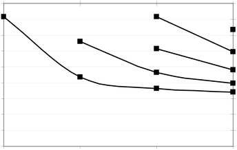
900 900 800 800 700 700 600 600
(meV) (meV)
500 500 E m n E m n 400 400 300 300 200 200 100 100 0 0
5 1 0 1 5 2 0
2a (nm)
Figure 7.2 Figure showing dependence of energy of transmission minima on tunnel barrier width 2a. For Al content x = 0.4 of Al x Ga 1−x As that corresponds to barrier height of 309 meV.
Chapter VII: Numerical investigation of parametric dependence of transmission minima
for non-tunneling regime of single rectangular tunnel barrier: Quantitative aspects
Table 7.18

x = 0.3, V 0 = 232 meV 2a (nm)
5 1 0 1 5 2 0
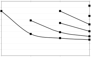
900 900 800 800 700 700 600 600
(meV) (meV)
500 500 E m n E m n 400 400 300 300 200 200 100 100 0 0
5 1 0 1 5 2 0
2a (nm)
Figure 7.3 Figure showing dependence of energy of transmission minima on tunnel barrier width 2a. For Al content x = 0.3 of Al x Ga 1−x As that corresponds to barrier height of 232 meV.
Oscillatory transmission through non-tunneling regime of single rectangular tunnel barrier:
Parametric dependence of maxima and of minima
Md Mahmud Hasan and Sujaul Chowdhury
Table 7.19

x = 0.2, V 0 = 155 meV 2a (nm)
5 1 0 1 5 2 0
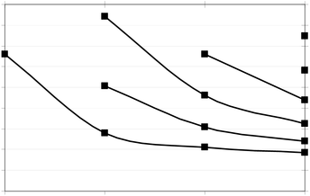
900 900 800 800 700 700 600 600
(meV) (meV)
500 500 E m n E m n 400 400 300 300 200 200 100 100 0 0
5 1 0 1 5 2 0
2a (nm)
Figure 7.4 Figure showing dependence of energy of transmission minima on tunnel barrier width 2a. For Al content x = 0.2 of Al x Ga 1−x As that corresponds to barrier height of 155 meV.
Chapter VII: Numerical investigation of parametric dependence of transmission minima
for non-tunneling regime of single rectangular tunnel barrier: Quantitative aspects
Table 7.20

x = 0.1, V 0 = 77 meV 2a (nm)
5 1 0 1 5 2 0
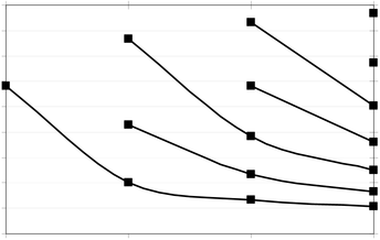
900 900 800 800 700 700 600 600
(meV) (meV)
500 500 E m n E m n 400 400 300 300 200 200 100 100 0 0
5 1 0 1 5 2 0
2a (nm)
Figure 7.5 Figure showing dependence of energy of transmission minima on tunnel barrier width 2a. For Al content x = 0.1 of Al x Ga 1−x As that corresponds to barrier height of 77 meV.
As Figure 7.2 to Figure 7.5 show, values of energy E mn of transmission minima decrease with increasing barrier width 2a in inverse square fashion. This we already explained in section 5.4.
Oscillatory transmission through non-tunneling regime of single rectangular tunnel barrier:
Parametric dependence of maxima and of minima
Md Mahmud Hasan and Sujaul Chowdhury
Table 7.21

w = 2a = 20 nm
V 0 (meV) 77 127 177 227 277
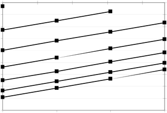
900 900 800 800 700 700 600 600
(meV) (meV)
500 500 E m n E m n 400 400 300 300 200 200 100 100 0 0
0 . 1 0 . 2 0 . 3 0 . 4
x
Figure 7.6 Figure showing dependence of energy of transmission minima on increasing Al content x of Al x Ga 1−x As that corresponds to increasing barrier height V 0 . For barrier width w = 2a = 20 nm.
Chapter VII: Numerical investigation of parametric dependence of transmission minima
for non-tunneling regime of single rectangular tunnel barrier: Quantitative aspects
Table 7.22

w = 2a = 15 nm
V 0 (meV) 77 127 177 227 277
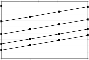
900 900 800 800 700 700 600 600
(meV) (meV)
500 500 E m n E m n 400 400 300 300 200 200 100 100 0 0
0 . 1 0 . 2 0 . 3 0 . 4
x
Figure 7.7 Figure showing dependence of energy of transmission minima on increasing Al content x of Al x Ga 1−x As that corresponds to increasing barrier height V 0 . For barrier width w = 2a = 15 nm.
Oscillatory transmission through non-tunneling regime of single rectangular tunnel barrier:
Parametric dependence of maxima and of minima
Md Mahmud Hasan and Sujaul Chowdhury
Table 7.23

w = 2a = 10 nm
V 0 (meV) 77 127 177 227 277
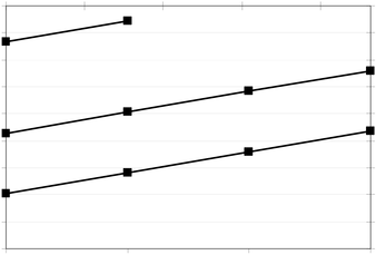
900 900 800 800 700 700 600 600
(meV) (meV)
500 500 E m n E m n 400 400 300 300 200 200 100 100 0 0
0 . 1 0 . 2 0 . 3 0 . 4
x
Figure 7.8 Figure showing dependence of energy of transmission minima on increasing Al content x of Al x Ga 1−x As that corresponds to increasing barrier height V 0 . For barrier width w = 2a = 10 nm.
Chapter VII: Numerical investigation of parametric dependence of transmission minima
for non-tunneling regime of single rectangular tunnel barrier: Quantitative aspects
Table 7.24

w = 2a = 5 nm
V 0 (meV) 77 127 177 227 277
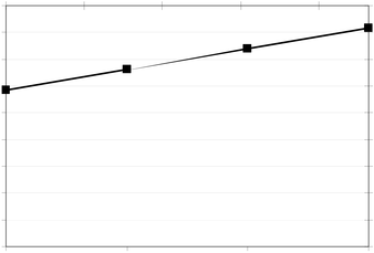
900 900 800 800 700 700 600 600
(meV) (meV)
500 500 E m n E m n 400 400 300 300 200 200 100 100 0 0
0 . 1 0 . 2 0 . 3 0 . 4
x
Figure 7.9 Figure showing dependence of energy of transmission minima on increasing Al content x of Al x Ga 1−x As that corresponds to increasing barrier height V 0 . For barrier width w = 2a = 5 nm.
As Figure 7.6 to Figure 7.9 show, energy E mn of transmission minima do not change with increasing Al content x of Al x Ga 1−x As that corresponds to increasing barrier height. This we already explained in section 5.3.
Oscillatory transmission through non-tunneling regime of single rectangular tunnel barrier:
Parametric dependence of maxima and of minima
Md Mahmud Hasan and Sujaul Chowdhury
References
[1] Sujaul Chowdhury "Quantum Mechanics: Textbook for Physics Honours" To be published 2012 [2] Sujaul Chowdhury "Nanostructure Physics and Microelectronics: Textbook for M.S. in Physics" To be published 2012
Monographs: ISBN: 978-3838368436, 978-3838373829, 978-3838375700, 978-3838376783, 978-3838377469, 978-3838378114, 978-3639334098, 978-3639337242, 978-3838394930 978-3659169397
References of
Oscillatory transmission through non-tunneling regime of single rectangular tunnel barrier:
Parametric dependence of maxima and of minima
Md Mahmud Hasan and Sujaul Chowdhury
For further studies of non-tunneling regime of nanostructures, one can read the following:
[3] Jian-Ping Peng, Yao-Ming Mu, and Xue-Chu Shen; Journal of Applied Physics 73 (1993) 989 [4] Marcello Colocci, Juan Martinez-Pastor, and Massimo Gurioli; Physical Review B 48 (1993) 8089 [5] C. D. Lee, J. S. Son, J. Y. Leem, and S. K. Noh, Kyu-Seok Lee, C. Lee, I. S. Hwang, and H. Y. Park; Physical Review B 54 (1996) 1541 [6] W. Lu, Y. M. Mu, X. Q. Liu, X. S. Chen, M. F. Wan, G. L. Shi, Y. M. Qiao, and S. C. Shen, Y. Fu and M. Willander; Physical Review B 57 (1998) 9787 [7] W. Trzeciakowski, D. Sahu, and Thomas F. George; Physical Review B 40 (1989) 6058 [8] S. Fafard; Physical Review B 46 (1992) 4659 [9] Witold Trzeciakowski and Massimo Gurioli; Journal of Physics: Condensed Matter 5 (1993) 105 [10] Witold Trzeciakowski and Massimo Gurioli; Journal of Physics: Condensed Matter 5 (1993) 1701 [11] R. Ferreira and G. Bastard; Nanoscale Res Lett 1 (2006) 1:120-136 [12] G. Bastard; Physical Review B 30 (1984) 3547 [13] G. Bastard; Superlattices and Microstructures, 1 (1985) 265 [14] G. Bastard, U.O. Ziemelis, C. Delalande, M. Voos, A.C. Gossard and W. Wiegmann; Solid State Communications 49 (1984) 671 [15] M Heiblum, M V Fischetti, W P Dumke, D J Frank, I M Anderson, C M Knoedler, L Osterling; Physical Review Letters 58 (1987) 816
- Quote paper
- Sujaul Chowdhury (Author)Mahmud Hasan (Author), 2013, Oscillatory transmission through non-tunneling regime of single rectangular tunnel barrier, Munich, GRIN Verlag, https://www.grin.com/document/210986
Similar texts


Publish now - it's free

Comments